
An electric current is a flow of electric charge. In electric circuits this charge is often carried by moving electrons in a wire. It can also be carried by ions in an electrolyte, or by both ions and electrons such as in an ionised gas (plasma).
Microelectronics is a subfield of electronics. As the name suggests, microelectronics relates to the study and manufacture of very small electronic designs and components. Usually, but not always, this means micrometre-scale or smaller. These devices are typically made from semiconductor materials. Many components of normal electronic design are available in a microelectronic equivalent. These include transistors, capacitors, inductors, resistors, diodes and (naturally) insulators and conductors can all be found in microelectronic devices. Unique wiring techniques such as wire bonding are also often used in microelectronics because of the unusually small size of the components, leads and pads. This technique requires specialized equipment and is expensive.

Semiconductor device fabrication is the process used to create the integrated circuits that are present in everyday electrical and electronic devices. It is a multiple-step sequence of photolithographic and chemical processing steps during which electronic circuits are gradually created on a wafer made of pure semiconducting material. Silicon is almost always used, but various compound semiconductors are used for specialized applications.
In solid-state physics, the work function is the minimum thermodynamic work needed to remove an electron from a solid to a point in the vacuum immediately outside the solid surface. Here "immediately" means that the final electron position is far from the surface on the atomic scale, but still too close to the solid to be influenced by ambient electric fields in the vacuum.
The work function is not a characteristic of a bulk material, but rather a property of the surface of the material.

The electrical resistance of an object is a measure of its opposition to the flow of electric current. The inverse quantity is electrical conductance, and is the ease with which an electric current passes. Electrical resistance shares some conceptual parallels with the notion of mechanical friction. The SI unit of electrical resistance is the ohm (Ω), while electrical conductance is measured in siemens (S).
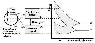
In solid-state physics, a band gap, also called an energy gap or bandgap, is an energy range in a solid where no electron states can exist. In graphs of the electronic band structure of solids, the band gap generally refers to the energy difference between the top of the valence band and the bottom of the conduction band in insulators and semiconductors. It is the energy required to promote a valence electron bound to an atom to become a conduction electron, which is free to move within the crystal lattice and serve as a charge carrier to conduct electric current. It is closely related to the HOMO/LUMO gap in chemistry. If the valence band is completely full and the conduction band is completely empty, then electrons cannot move in the solid; however, if some electrons transfer from the valence to the conduction band, then current can flow. Therefore, the band gap is a major factor determining the electrical conductivity of a solid. Substances with large band gaps are generally insulators, those with smaller band gaps are semiconductors, while conductors either have very small band gaps or none, because the valence and conduction bands overlap.
The Fermi level chemical potential for electrons of a body is the thermodynamic work required to add one electron to the body. It is a thermodynamic quantity usually denoted by µ or EF
for brevity. The Fermi level does not include the work required to remove the electron from wherever it came from.
A precise understanding of the Fermi level—how it relates to electronic band structure in determining electronic properties, how it relates to the voltage and flow of charge in an electronic circuit—is essential to an understanding of solid-state physics.
In physics, a charge carrier is a particle or quasiparticle that is free to move, carrying an electric charge, especially the particles that carry electric charges in electrical conductors. Examples are electrons, ions and holes. In a conducting medium, an electric field can exert force on these free particles, causing a net motion of the particles through the medium; this is what constitutes an electric current. In different conducting media, different particles serve to carry charge:

Conductive polymers or, more precisely, intrinsically conducting polymers (ICPs) are organic polymers that conduct electricity. Such compounds may have metallic conductivity or can be semiconductors. The biggest advantage of conductive polymers is their processability, mainly by dispersion. Conductive polymers are generally not thermoplastics, i.e., they are not thermoformable. But, like insulating polymers, they are organic materials. They can offer high electrical conductivity but do not show similar mechanical properties to other commercially available polymers. The electrical properties can be fine-tuned using the methods of organic synthesis and by advanced dispersion techniques.
KPR, originally known as Kodak Photoresist, is a photosensitive material used in photoengraving, Photogravure and photolithography. Once dried KPR can be dissolved by several solvents but after exposure to strong ultraviolet light it hardens and becomes insoluble by some of these solvents. It is also resistant to acid, ferric chloride and other chemicals used to etch metals.

Lawrence Roger 'Larry' Fast is a synthesizer expert and composer. He is best known for Synergy, his 1975–1987 series of synthesizer music albums, and for his contributions to a number of popular music acts, including Peter Gabriel, Foreigner, Nektar, and Hall & Oates.

Solid-state electronics means semiconductor electronics; electronic equipment using semiconductor devices such as semiconductor diodes, transistors, and integrated circuits (ICs). The term is also used for devices in which semiconductor electronics which have no moving parts replace devices with moving parts, such as the solid-state relay in which transistor switches are used in place of a moving-arm electromechanical relay, or the solid state disk (SSD) a type of semiconductor memory used in computers to replace hard disk drives, which store data on a rotating disk.
An ohmic contact is a non-rectifying electrical junction: a junction between two conductors that has a linear current–voltage (I-V) curve as with Ohm's law. Low resistance ohmic contacts are used to allow charge to flow easily in both directions between the two conductors, without blocking due to rectification or excess power dissipation due to voltage thresholds.

In solid-state physics of semiconductors, a band diagram is a diagram plotting various key electron energy levels as a function of some spatial dimension, which is often denoted x. These diagrams help to explain the operation of many kinds of semiconductor devices and to visualize how bands change with position. The bands may be coloured to distinguish level filling.

The Semi-Conductor Laboratory, Mohali (SCL) is a research institute of the Department of Space, Government of India. Its aims include research and development in the field of semiconductor technology.
Chenming Calvin Hu is an electronic engineer who specializes in microelectronics. He is TSMC Distinguished Professor Emeritus in the electronic engineering and computer science department of the University of California, Berkeley, in the United States. In 2009, the Institute of Electrical and Electronics Engineers described him as a “microelectronics visionary … whose seminal work on metal-oxide semiconductor MOS reliability and device modeling has had enormous impact on the continued scaling of electronic devices”.

John Robertson FRS is a Professor of Electronics, in the Department of Engineering at the University of Cambridge. He is a leading specialist in the theory of amorphous carbon and related materials.

In solid-state physics, the valence band and conduction band are the bands closest to the Fermi level and thus determine the electrical conductivity of the solid. In non-metals, the valence band is the highest range of electron energies in which electrons are normally present at absolute zero temperature, while the conduction band is the lowest range of vacant electronic states. On a graph of the electronic band structure of a material, the valence band is located below the Fermi level, while the conduction band is located above it.