
A circuit diagram is a graphical representation of an electrical circuit. A pictorial circuit diagram uses simple images of components, while a schematic diagram shows the components and interconnections of the circuit using standardized symbolic representations. The presentation of the interconnections between circuit components in the schematic diagram does not necessarily correspond to the physical arrangements in the finished device.

The Gerber format is an open ASCII vector format for 2D binary images. It is the de facto standard used by printed circuit board (PCB) industry software to describe the printed circuit board images: copper layers, solder mask, legend, drill data, etc.

Printed circuit board milling is the process of removing areas of copper from a sheet of printed circuit board material to recreate the pads, signal traces and structures according to patterns from a digital circuit board plan known as a layout file. Similar to the more common and well known chemical PCB etch process, the PCB milling process is subtractive: material is removed to create the electrical isolation and ground planes required. However, unlike the chemical etch process, PCB milling is typically a non-chemical process and as such it can be completed in a typical office or lab environment without exposure to hazardous chemicals. High quality circuit boards can be produced using either process. In the case of PCB milling, the quality of a circuit board is chiefly determined by the system's true, or weighted, milling accuracy and control as well as the condition of the milling bits and their respective feed/rotational speeds. By contrast, in the chemical etch process, the quality of a circuit board depends on the accuracy and/or quality of the photomasking and the state of the etching chemicals.
In telecommunication, a microstrip antenna usually means an antenna fabriciated using microstrip techniques on a printed circuit board (PCB). It is a kind of internal antenna. They are mostly used at microwave frequencies. An individual microstrip antenna consists of a patch of metal foil of various shapes on the surface of a PCB, with a metal foil ground plane on the other side of the board. Most microstrip antennas consist of multiple patches in a two-dimensional array. The antenna is usually connected to the transmitter or receiver through foil microstrip transmission lines. The radio frequency current is applied between the antenna and ground plane. Microstrip antennas have become very popular in recent decades due to their thin planar profile which can be incorporated into the surfaces of consumer products, aircraft and missiles; their ease of fabrication using printed circuit techniques; the ease of integrating the antenna on the same board with the rest of the circuit, and the possibility of adding active devices such as microwave integrated circuits to the antenna itself to make active antennas.
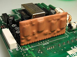
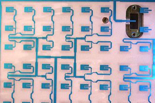
A hybrid integrated circuit (HIC), hybrid microcircuit, hybrid circuit or simply hybrid is a miniaturized electronic circuit constructed of individual devices, such as semiconductor devices and passive components, bonded to a substrate or printed circuit board (PCB). A PCB having components on a Printed Wiring Board (PWB) is not considered a hybrid circuit according to the definition of MIL-PRF-38534.
Electronics manufacturing services (EMS) is a term used for companies that design, manufacture, test, distribute, and provide return/repair services for electronic components and assemblies for original equipment manufacturers (OEMs). The concept is also referred to as electronics contract manufacturing (ECM).

In electronics, the term copper pour refers to an area on a printed circuit board filled with copper. Copper pour is commonly used to create a ground plane. Another reason for using copper pour is to reduce the amount of etching fluid used during manufacturing.
Automated optical inspection (AOI) is an automated visual inspection of printed circuit board (PCB) manufacture where a camera autonomously scans the device under test for both catastrophic failure and quality defects. It is commonly used in the manufacturing process because it is a non-contact test method. It is implemented at many stages through the manufacturing process including bare board inspection, solder paste inspection (SPI), pre-reflow and post-reflow as well as other stages.
In-circuit test (ICT) is an example of white box testing where an electrical probe tests a populated printed circuit board (PCB), checking for shorts, opens, resistance, capacitance, and other basic quantities which will show whether the assembly was correctly fabricated. It may be performed with a bed of nails type test fixture and specialist test equipment, or with a fixtureless in-circuit test setup.
Defence Electronics & Research Laboratory (DLRL) is a laboratory of the Defence Research & Development Organization (DRDO). Located in Hyderabad, it is actively involved in the design and development of integrated Electronic Warfare systems for the Indian Armed Forces.
CR-5000 is Zuken's design suite for electronics systems and printed circuit boards aimed at the enterprise market. It was developed to tackle complex design needs that involve managing the complete development and manufacturing preparation process on an enterprise-wide scale. CR-5000 offers relevant functionality for the design of complex and high-speed boards, addressing design challenges such as signal integrity and electromagnetic compatibility.
Microvias are used as the interconnects between layers in high density interconnect (HDI) substrates and printed circuit boards (PCBs) to accommodate the high input/output (I/O) density of advanced packages. Driven by portability and wireless communications, the electronics industry strives to produce affordable, light, and reliable products with increased functionality. At the electronic component level, this translates to components with increased I/Os with smaller footprint areas, and on the printed circuit board and package substrate level, to the use of high density interconnects (HDIs).

Printed Circuit Corporation (PCC) was founded in 1961 and was a contract printed circuit board manufacturer located in Woburn, Massachusetts.. PCC provided its products to companies in the electronics, instrumentation, medical, telecommunication, and automotive industries. The majority of the boards produced were multilayer.
Comparison of electronic design automation (EDA) software
Coupon may refer to the following:

ODB++ is a proprietary CAD-to-CAM data exchange format used in the design and manufacture of electronic devices. Its purpose is to exchange printed circuit board design information between design and manufacturing and between design tools from different EDA/ECAD vendors. It was originally developed by Valor Computerized Systems, Ltd. as the job description format for their CAM system.
Stencil printing is the process of depositing solder paste on the printed wiring boards (PWBs) to establish electrical connections. It is immediately followed by the component placement stage. The equipment and materials used in this stage are stencil, solder paste, and a printer.
In electronics, a cross section, cross-section, or microsection, is a prepared electronics sample that allows analysis at a plane that cuts through the sample. It is a destructive technique requiring that a portion of the sample be cut or ground away to expose the internal plane for analysis. They are commonly prepared for research, manufacturing quality assurance, supplier conformity, and failure analysis. Printed wiring boards (PWBs) and electronic components and their solder joints are common cross sectioned samples. The features of interest to be analyzed in cross section can be nanometer-scale metal and dielectric layers in semiconductors up to macroscopic features such as the amount of solder that has filled into a large, 0.125in (3.18mm) diameter plated through hole.
Specctra is a commercial PCB auto-router originally developed by John F. Cooper and David Chyan of Cooper & Chyan Technology, Inc. (CCT) in 1989. The company and product were taken over by Cadence Design Systems in May 1997. Since its integration into Cadence's Allegro PCB Editor, the name of the router is Allegro PCB Router. The latest version is 17.2.
