Sigma and pi bonds in graphene. Sigma bonds result from an overlap of sp hybrid orbitals, whereas pi bonds emerge from tunneling between the protruding pz orbitals. For clarity, only one pz orbital is shown with its three nearest neighbors.
Graphene is a semimetal whose conduction and valence bands meet at the Dirac points, which are six locations in momentum space, the vertices of its hexagonal Brillouin zone, divided into two non-equivalent sets of three points. The two sets are labeled K and K'. The sets give graphene a valley degeneracy of gv = 2. By contrast, for traditional semiconductors the primary point of interest is generally Γ, where momentum is zero.[1] Four electronic properties separate it from other condensed matter systems.
Electrons propagating through graphene's honeycomb lattice effectively lose their mass, producing quasi-particles that are described by a 2D analogue of the Dirac equation rather than the Schrödinger equation for spin-1⁄2 particles.[2][3]
Dispersion relation
Electronic band structure of graphene. Valence and conduction bands meet at the six vertices of the hexagonal Brillouin zone and form linearly dispersing Dirac cones.
When atoms are placed onto the graphene hexagonal lattice, the overlap between the pz(π) orbitals and the s or the px and py orbitals is zero by symmetry. The pz electrons forming the π bands in graphene can be treated independently. Within this π-band approximation, using a conventional tight-binding model, the dispersion relation (restricted to first-nearest-neighbor interactions only) that produces energy of the electrons with wave vector is[4][5]
with the nearest-neighbor (π orbitals) hopping energy γ0 ≈ 2.8eV and the lattice constanta ≈ 2.46Å. The conduction and valence bands, respectively, correspond to the different signs. With one pz electron per atom in this model the valence band is fully occupied, while the conduction band is vacant. The two bands touch at the zone corners (the K point in the Brillouin zone), where there is a zero density of states but no band gap. The graphene sheet thus displays a semimetallic (or zero-gap semiconductor) character. Two of the six Dirac points are independent, while the rest are equivalent by symmetry. In the vicinity of the K-points the energy depends linearly on the wave vector, similar to a relativistic particle.[4][6] Since an elementary cell of the lattice has a basis of two atoms, the wave function has an effective 2-spinor structure.
As a consequence, at low energies, even neglecting the true spin, the electrons can be described by an equation that is formally equivalent to the massless Dirac equation. Hence, the electrons and holes are called Dirac fermions.[4] This pseudo-relativistic description is restricted to the chiral limit, i.e., to vanishing rest mass M0, which leads to additional features:[4][7]
Here vF ~ 106m/s (.003 c) is the Fermi velocity in graphene, which replaces the velocity of light in the Dirac theory; is the vector of the Pauli matrices; is the two-component wave function of the electrons and E is their energy.[2]
The equation describing the electrons' linear dispersion relation is
where the wavevector is measured from the Dirac points (the zero of energy is chosen here to coincide with the Dirac points). The equation uses a pseudospin matrix formula that describes two sublattices of the honeycomb lattice.[6]
'Massive' electrons
Graphene's unit cell has two identical carbon atoms and two zero-energy states: one in which the electron resides on atom A, the other in which the electron resides on atom B. However, if the two atoms in the unit cell are not identical, the situation changes. Hunt et al. showed that placing hexagonal boron nitride (h-BN) in contact with graphene can alter the potential felt at atom A versus atom B enough that the electrons develop a mass and accompanying band gap of about 30 meV [0.03 Electron Volt (eV)].[8]
The mass can be positive or negative. An arrangement that slightly raises the energy of an electron on atom A relative to atom B gives it a positive mass, while an arrangement that raises the energy of atom B produces a negative electron mass. The two versions behave alike and are indistinguishable via optical spectroscopy. An electron traveling from a positive-mass region to a negative-mass region must cross an intermediate region where its mass once again becomes zero. This region is gapless and therefore metallic. Metallic modes bounding semiconducting regions of opposite-sign mass is a hallmark of a topological phase and display much the same physics as topological insulators.[8]
If the mass in graphene can be controlled, electrons can be confined to massless regions by surrounding them with massive regions, allowing the patterning of quantum dots, wires and other mesoscopic structures. It also produces one-dimensional conductors along the boundary. These wires would be protected against backscattering and could carry currents without dissipation.[8]
Graphene displays remarkable electron mobility at room temperature, with reported values in excess of 15000cm2⋅V−1⋅s−1.[9] Hole and electron mobilities were expected to be nearly identical.[3] The mobility is nearly independent of temperature between 10K and 100K,[10][11][12] which implies that the dominant scattering mechanism is defect scattering. Scattering by graphene's acoustic phonons intrinsically limits room temperature mobility to 200000cm2⋅V−1⋅s−1 at a carrier density of 1012cm−2,[12][13]10×106 times greater than copper.[14]
The corresponding resistivity of graphene sheets would be 10−6Ω⋅cm. This is less than the resistivity of silver, the lowest otherwise known at room temperature.[15] However, on SiO 2 substrates, scattering of electrons by optical phonons of the substrate is a larger effect than scattering by graphene's own phonons. This limits mobility to 40000cm2⋅V−1⋅s−1.[12]
Charge transport is affected by adsorption of contaminants such as water and oxygen molecules. This leads to non-repetitive and large hysteresis I-V characteristics. Researchers must carry out electrical measurements in vacuum. Graphene surfaces can be protected by a coating with materials such as SiN, PMMA and h-BN. In January 2015, the first stable graphene device operation in air over several weeks was reported, for graphene whose surface was protected by aluminum oxide.[16][17] In 2015 lithium-coated graphene was observed to exhibit superconductivity[18] and in 2017 evidence for unconventional superconductivity was demonstrated in single layer graphene placed on the electron-doped (non-chiral) d-wave superconductor Pr2−xCexCuO4 (PCCO).[19]
Electrical resistance in 40-nanometer-wide nanoribbons of epitaxial graphene changes in discrete steps. The ribbons' conductance exceeds predictions by a factor of 10. The ribbons can act more like optical waveguides or quantum dots, allowing electrons to flow smoothly along the ribbon edges. In copper, resistance increases in proportion to length as electrons encounter impurities.[20][21]
Transport is dominated by two modes. One is ballistic and temperature independent, while the other is thermally activated. Ballistic electrons resemble those in cylindrical carbon nanotubes. At room temperature, resistance increases abruptly at a particular length—the ballistic mode at 16 micrometres and the other at 160 nanometres.[20]
Graphene electrons can cover micrometer distances without scattering, even at room temperature.[2]
Despite zero carrier density near the Dirac points, graphene exhibits a minimum conductivity on the order of . The origin of this minimum conductivity is unclear. However, rippling of the graphene sheet or ionized impurities in the SiO 2 substrate may lead to local puddles of carriers that allow conduction.[3] Several theories suggest that the minimum conductivity should be ; however, most measurements are of order or greater[9] and depend on impurity concentration.[22]
Near zero carrier density graphene exhibits positive photoconductivity and negative photoconductivity at high carrier density. This is governed by the interplay between photoinduced changes of both the Drude weight and the carrier scattering rate.[23]
Graphene doped with various gaseous species (both acceptors and donors) can be returned to an undoped state by gentle heating in vacuum.[22][24] Even for dopant concentrations in excess of 1012 cm−2 carrier mobility exhibits no observable change.[24] Graphene doped with potassium in ultra-high vacuum at low temperature can reduce mobility 20-fold.[22][25] The mobility reduction is reversible on removing the potassium.
Due to graphene's two dimensions, charge fractionalization (where the apparent charge of individual pseudoparticles in low-dimensional systems is less than a single quantum[26]) is thought to occur. It may therefore be a suitable material for constructing quantum computers[27] using anyonic circuits.[28]
In 2018, superconductivity was reported in twisted bilayer graphene.
Excitonic properties
First-principle calculations with quasiparticle corrections and many-body effects explore the electronic and optical properties of graphene-based materials. The approach is described as three stages.[29] With GW calculation, the properties of graphene-based materials are accurately investigated, including bulk graphene,[30]nanoribbons,[31] edge and surface functionalized armchair oribbons,[32] hydrogen saturated armchair ribbons,[33]Josephson effect in graphene SNS junctions with single localized defect[34] and armchair ribbon scaling properties.[35]
Magnetic properties
In 2014 researchers magnetized graphene by placing it on an atomically smooth layer of magnetic yttrium iron garnet. The graphene's electronic properties were unaffected. Prior approaches involved doping.[36] The dopant's presence negatively affected its electronic properties.[37]
Strong magnetic fields
In magnetic fields of ≈10 tesla, additional plateaus of Hall conductivity at with are observed.[38] The observation of a plateau at [39] and the fractional quantum Hall effect at were reported.[39][40]
These observations with indicate that the four-fold degeneracy (two valley and two spin degrees of freedom) of the Landau energy levels is partially or completely lifted.[41] One hypothesis is that the magnetic catalysis of symmetry breaking is responsible for lifting the degeneracy.[citation needed]
Spin transport
Graphene is claimed to be an ideal material for spintronics due to its small spin-orbit interaction and the near absence of nuclear magnetic moments in carbon (as well as a weak hyperfine interaction). Electrical spin current injection and detection has been demonstrated up to room temperature.[42][43][44] Spin coherence length above 1 micrometre at room temperature was observed,[42] and control of the spin current polarity with an electrical gate was observed at low temperature.[43]
Spintronic and magnetic properties can be present in graphene simultaneously.[45] Low-defect graphene nanomeshes manufactured using a non-lithographic method exhibit large-amplitude ferromagnetism even at room temperature. Additionally a spin pumping effect is found for fields applied in parallel with the planes of few-layer ferromagnetic nanomeshes, while a magnetoresistance hysteresis loop is observed under perpendicular fields.[citation needed]
Dirac fluid
Charged particles in high-purity graphene behave as a strongly interacting, quasi-relativistic plasma. The particles move in a fluid-like manner, traveling along a single path and interacting with high frequency. The behavior was observed in a graphene sheet faced on both sides with a h-BN crystal sheet.[46]
Graphene shows the quantum Hall effect with respect to conductivity quantization: the effect is anomalous in that the sequence of steps is shifted by 1/2 with respect to the standard sequence and with an additional factor of 4. Graphene's Hall conductivity is , where N is the Landau level and the double valley and double spin degeneracies give the factor of 4.[9] These anomalies are present at room temperature, i.e. at roughly 20°C (293K).[10]
This behavior is a direct result of graphene's massless Dirac electrons. In a magnetic field, their spectrum has a Landau level with energy precisely at the Dirac point. This level is a consequence of the Atiyah–Singer index theorem and is half-filled in neutral graphene,[4] leading to the "+1/2" in the Hall conductivity.[47] Bilayer graphene also shows the quantum Hall effect, but with only one of the two anomalies (i.e. ). In the second anomaly, the first plateau at N=0 is absent, indicating that bilayer graphene stays metallic at the neutrality point.[9]
Unlike normal metals, graphene's longitudinal resistance shows maxima rather than minima for integral values of the Landau filling factor in measurements of the Shubnikov–de Haas oscillations, whereby the term integral quantum Hall effect. These oscillations show a phase shift of π, known as Berry's phase.[10][3] Berry's phase arises due to the zero effective carrier mass near the Dirac points.[48] The temperature dependence of the oscillations reveals that the carriers have a non-zero cyclotron mass, despite their zero effective mass.[10]
Graphene samples prepared on nickel films, and on both the silicon face and carbon face of silicon carbide, show the anomalous effect directly in electrical measurements.[49][50][51][52][53][54] Graphitic layers on the carbon face of silicon carbide show a clear Dirac spectrum in angle-resolved photoemission experiments. The effect is observed in cyclotron resonance and tunneling experiments.[55]
Casimir effect
The Casimir effect is an interaction between disjoint neutral bodies provoked by the fluctuations of the electrodynamical vacuum. Mathematically it can be explained by considering the normal modes of electromagnetic fields, which explicitly depend on the boundary (or matching) conditions on the interacting bodies' surfaces. Since graphene/electromagnetic field interaction is strong for a one-atom-thick material, the Casimir effect is of interest.[56][57]
Van der Waals force
The Van der Waals force (or dispersion force) is also unusual, obeying an inverse cubic, asymptotic power law in contrast to the usual inverse quartic.[58]
Effect of substrate
The electronic properties of graphene are significantly influenced by the supporting substrate.[59][60] The Si(100)/H surface does not perturb graphene's electronic properties, whereas the interaction between it and the clean Si(100) surface changes its electronic states significantly. This effect results from the covalent bonding between C and surface Si atoms, modifying the π-orbital network of the graphene layer. The local density of states shows that the bonded C and Si surface states are highly disturbed near the Fermi energy.
If the in-plane direction is confined, in which case it is referred to as a nanoribbon, its electronic structure is different. If it is "zig-zag" (diagram), the bandgap is zero. If it is "armchair" (diagram), the bandgap is non-zero (see figure).
GNRband structure for zig-zag orientation. Tightbinding calculations show that zig-zag orientation is always metallic.
GNRband structure for armchair orientation. Tightbinding calculations show that armchair orientation can be semiconducting or metallic depending on width (chirality).
Related Research Articles
The quantum Hall effect is a quantized version of the Hall effect which is observed in two-dimensional electron systems subjected to low temperatures and strong magnetic fields, in which the Hall resistance Rxy exhibits steps that take on the quantized values
In physics, the Kondo effect describes the scattering of conduction electrons in a metal due to magnetic impurities, resulting in a characteristic change i.e. a minimum in electrical resistivity with temperature. The cause of the effect was first explained by Jun Kondo, who applied third-order perturbation theory to the problem to account for scattering of s-orbital conduction electrons off d-orbital electrons localized at impurities. Kondo's calculation predicted that the scattering rate and the resulting part of the resistivity should increase logarithmically as the temperature approaches 0 K. Experiments in the 1960s by Myriam Sarachik at Bell Laboratories provided the first data that confirmed the Kondo effect. Extended to a lattice of magnetic impurities, the Kondo effect likely explains the formation of heavy fermions and Kondo insulators in intermetallic compounds, especially those involving rare earth elements such as cerium, praseodymium, and ytterbium, and actinide elements such as uranium. The Kondo effect has also been observed in quantum dot systems.
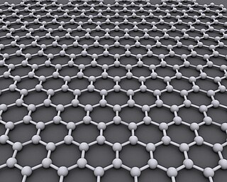
Graphene is an allotrope of carbon consisting of a single layer of atoms arranged in a hexagonal lattice nanostructure. The name is derived from "graphite" and the suffix -ene, reflecting the fact that the graphite allotrope of carbon contains numerous double bonds.
In physics, the zitterbewegung (German pronunciation:[ˈtsɪtɐ.bəˌveːɡʊŋ], from German zittern 'to tremble, jitter', and Bewegung 'motion') is the theoretical prediction of a rapid oscillatory motion of elementary particles that obey relativistic wave equations. This prediction was first discussed by Gregory Breit in 1928 and later by Erwin Schrödinger in 1930 as a result of analysis of the wave packet solutions of the Dirac equation for relativistic electrons in free space, in which an interference between positive and negative energy states produces an apparent fluctuation (up to the speed of light) of the position of an electron around the median, with an angular frequency of 2mc2/ℏ, or approximately 1.6×10²¹ radians per second.
A two-dimensional electron gas (2DEG) is a scientific model in solid-state physics. It is an electron gas that is free to move in two dimensions, but tightly confined in the third. This tight confinement leads to quantized energy levels for motion in the third direction, which can then be ignored for most problems. Thus the electrons appear to be a 2D sheet embedded in a 3D world. The analogous construct of holes is called a two-dimensional hole gas (2DHG), and such systems have many useful and interesting properties.
A Majorana fermion, also referred to as a Majorana particle, is a fermion that is its own antiparticle. They were hypothesised by Ettore Majorana in 1937. The term is sometimes used in opposition to a Dirac fermion, which describes fermions that are not their own antiparticles.
A quantum point contact (QPC) is a narrow constriction between two wide electrically conducting regions, of a width comparable to the electronic wavelength.
Graphene nanoribbons are strips of graphene with width less than 100 nm. Graphene ribbons were introduced as a theoretical model by Mitsutaka Fujita and coauthors to examine the edge and nanoscale size effect in graphene.
The quantum spin Hall state is a state of matter proposed to exist in special, two-dimensional semiconductors that have a quantized spin-Hall conductance and a vanishing charge-Hall conductance. The quantum spin Hall state of matter is the cousin of the integer quantum Hall state, and that does not require the application of a large magnetic field. The quantum spin Hall state does not break charge conservation symmetry and spin- conservation symmetry.
Subir Sachdev is Herchel Smith Professor of Physics at Harvard University specializing in condensed matter. He was elected to the U.S. National Academy of Sciences in 2014, received the Lars Onsager Prize from the American Physical Society and the Dirac Medal from the ICTP in 2018, and was elected Foreign Member of the Royal Society ForMemRS in 2023. He was a co-editor of the Annual Review of Condensed Matter Physics 2017–2019, and is Editor-in-Chief of Reports on Progress in Physics 2022-.
A topological insulator is a material whose interior behaves as an electrical insulator while its surface behaves as an electrical conductor, meaning that electrons can only move along the surface of the material.
Silicene is a two-dimensional allotrope of silicon, with a hexagonal honeycomb structure similar to that of graphene. Contrary to graphene, silicene is not flat, but has a periodically buckled topology; the coupling between layers in silicene is much stronger than in multilayered graphene; and the oxidized form of silicene, 2D silica, has a very different chemical structure from graphene oxide.
Bilayer graphene is a material consisting of two layers of graphene. One of the first reports of bilayer graphene was in the seminal 2004 Science paper by Geim and colleagues, in which they described devices "which contained just one, two, or three atomic layers"
Bose–Einstein condensation can occur in quasiparticles, particles that are effective descriptions of collective excitations in materials. Some have integer spins and can be expected to obey Bose–Einstein statistics like traditional particles. Conditions for condensation of various quasiparticles have been predicted and observed. The topic continues to be an active field of study.
Valleytronics is an experimental area in semiconductors that exploits local extrema ("valleys") in the electronic band structure. Certain semiconductors have multiple "valleys" in the electronic band structure of the first Brillouin zone, and are known as multivalley semiconductors. Valleytronics is the technology of control over the valley degree of freedom, a local maximum/minimum on the valence/conduction band, of such multivalley semiconductors.
In physics, Dirac cones are features that occur in some electronic band structures that describe unusual electron transport properties of materials like graphene and topological insulators. In these materials, at energies near the Fermi level, the valence band and conduction band take the shape of the upper and lower halves of a conical surface, meeting at what are called Dirac points.
Single-layer graphene was first unambiguously produced and identified in 2004, by the group of Andre Geim and Konstantin Novoselov, though they credit Hanns-Peter Boehm and his co-workers for the experimental discovery of graphene in 1962; while it had been explored theoretically by P. R. Wallace in 1947. Boehm et al. introduced the term graphene in 1986.
Spin squeezing is a quantum process that decreases the variance of one of the angular momentum components in an ensemble of particles with a spin. The quantum states obtained are called spin squeezed states. Such states have been proposed for quantum metrology, to allow a better precision for estimating a rotation angle than classical interferometers.
The term Dirac matter refers to a class of condensed matter systems which can be effectively described by the Dirac equation. Even though the Dirac equation itself was formulated for fermions, the quasi-particles present within Dirac matter can be of any statistics. As a consequence, Dirac matter can be distinguished in fermionic, bosonic or anyonic Dirac matter. Prominent examples of Dirac matter are graphene and other Dirac semimetals, topological insulators, Weyl semimetals, various high-temperature superconductors with -wave pairing and liquid helium-3. The effective theory of such systems is classified by a specific choice of the Dirac mass, the Dirac velocity, the gamma matrices and the space-time curvature. The universal treatment of the class of Dirac matter in terms of an effective theory leads to a common features with respect to the density of states, the heat capacity and impurity scattering.
Sung Ryul Eric Yang is a theoretical condensed matter physicist. He is a full professor in the Department of Physics of Korea University.
References
↑ Cooper, Daniel R.; D’Anjou, Benjamin; Ghattamaneni, Nageswara; Harack, Benjamin; Hilke, Michael; Horth, Alexandre; Majlis, Norberto; Massicotte, Mathieu; Vandsburger, Leron; Whiteway, Eric; Yu, Victor (3 November 2011). "Experimental Review of Graphene"(PDF). ISRN Condensed Matter Physics. 2012: 1–56. arXiv:1110.6557. doi:10.5402/2012/501686. S2CID78304205. Retrieved 30 August 2016.
↑ Akturk, A.; Goldsman, N. (2008). "Electron transport and full-band electron–phonon interactions in graphene". Journal of Applied Physics. 103 (5): 053702–053702–8. Bibcode:2008JAP...103e3702A. doi:10.1063/1.2890147.
↑ Kusmartsev, F. V.; Wu, W. M.; Pierpoint, M. P.; Yung, K. C. (2014). "Application of Graphene within Optoelectronic Devices and Transistors". arXiv:1406.0809 [cond-mat.mtrl-sci].
↑ Zhu, Xi; Su, Haibin (2010). "Excitons of Edge and Surface Functionalized Graphene Nanoribbons". J. Phys. Chem. C. 114 (41): 17257–17262. doi:10.1021/jp102341b.
↑ Kim, Kuen Soo; Zhao, Yue; Jang, Houk; Lee, Sang Yoon; Kim, Jong Min; Kim, Kwang S.; Ahn, Jong-Hyun; Kim, Philip; Choi, Jae-Young; Hong, Byung Hee (2009). "Large-scale pattern growth of graphene films for stretchable transparent electrodes". Nature. 457 (7230): 706–10. Bibcode:2009Natur.457..706K. doi:10.1038/nature07719. PMID19145232. S2CID4349731.
↑ Jobst, Johannes; Waldmann, Daniel; Speck, Florian; Hirner, Roland; Maude, Duncan K.; Seyller, Thomas; Weber, Heiko B. (2009). "How Graphene-like is Epitaxial Graphene? Quantum Oscillations and Quantum Hall Effect". Physical Review B. 81 (19): 195434. arXiv:0908.1900. Bibcode:2010PhRvB..81s5434J. doi:10.1103/PhysRevB.81.195434. S2CID118710923.
↑ Shen, T.; Gu, J.J.; Xu, M; Wu, Y.Q.; Bolen, M.L.; Capano, M.A.; Engel, L.W.; Ye, P.D. (2009). "Observation of quantum-Hall effect in gated epitaxial graphene grown on SiC (0001)". Applied Physics Letters. 95 (17): 172105. arXiv:0908.3822. Bibcode:2009ApPhL..95q2105S. doi:10.1063/1.3254329. S2CID9546283.
↑ Xu, Yang; He, K. T.; Schmucker, S. W.; Guo, Z.; Koepke, J. C.; Wood, J. D.; Lyding, J. W.; Aluru, N. R. (2011). "Inducing Electronic Changes in Graphene through Silicon (100) Substrate Modification". Nano Letters. 11 (7): 2735–2742. Bibcode:2011NanoL..11.2735X. doi:10.1021/nl201022t. PMID21661740.
This page is based on this Wikipedia article Text is available under the CC BY-SA 4.0 license; additional terms may apply. Images, videos and audio are available under their respective licenses.


 GNR band structure for zig-zag orientation. Tightbinding calculations show that zig-zag orientation is always metallic.
 GNR band structure for armchair orientation. Tightbinding calculations show that armchair orientation can be semiconducting or metallic depending on width (chirality).