
Electronics comprises the physics, engineering, technology and applications that deal with the emission, flow and control of electrons in vacuum and matter.

An integrated circuit or monolithic integrated circuit is a set of electronic circuits on one small flat piece of semiconductor material that is normally silicon. The integration of large numbers of tiny MOS transistors into a small chip results in circuits that are orders of magnitude smaller, faster, and less expensive than those constructed of discrete electronic components. The IC's mass production capability, reliability, and building-block approach to circuit design has ensured the rapid adoption of standardized ICs in place of designs using discrete transistors. ICs are now used in virtually all electronic equipment and have revolutionized the world of electronics. Computers, mobile phones, and other digital home appliances are now inextricable parts of the structure of modern societies, made possible by the small size and low cost of ICs.

Semiconductor device fabrication is the process used to manufacture semiconductor devices, typically the metal-oxide-semiconductor (MOS) devices used in the integrated circuit (IC) chips that are present in everyday electrical and electronic devices. It is a multiple-step sequence of photolithographic and chemical processing steps during which electronic circuits are gradually created on a wafer made of pure semiconducting material. Silicon is almost always used, but various compound semiconductors are used for specialized applications.
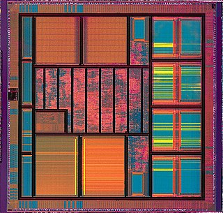
Very-large-scale integration (VLSI) is the process of creating an integrated circuit (IC) by combining millions of MOS transistors onto a single chip. VLSI began in the 1970s when MOS integrated circuit chips were widely adopted, enabling complex semiconductor and telecommunication technologies to be developed. The microprocessor and memory chips are VLSI devices. Before the introduction of VLSI technology, most ICs had a limited set of functions they could perform. An electronic circuit might consist of a CPU, ROM, RAM and other glue logic. VLSI lets IC designers add all of these into one chip.

The metal–oxide–semiconductor field-effect transistor (MOSFET, MOS-FET, or MOS FET), also known as the metal–oxide–silicon transistor (MOS transistor, or MOS), is a type of field-effect transistor that is fabricated by the controlled oxidation of a semiconductor, typically silicon. It has an insulated gate, whose voltage determines the conductivity of the device. This ability to change conductivity with the amount of applied voltage can be used for amplifying or switching electronic signals. It was invented by Egyptian engineer Mohamed M. Atalla and Korean engineer Dawon Kahng at Bell Labs in November 1959. The MOSFET is the basic building block of modern electronics, and the most widely manufactured device in history, with an estimated total of 13 sextillion (1.3 × 10²²) MOSFETs manufactured between 1960 and 2018.
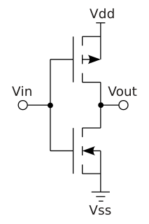
Complementary metal–oxide–semiconductor (CMOS), also known as complementary-symmetry metal–oxide–semiconductor (COS-MOS), is a type of MOSFET fabrication process that uses complementary and symmetrical pairs of p-type and n-type MOSFETs for logic functions. CMOS technology is used for constructing integrated circuits (ICs), including microprocessors, microcontrollers, memory chips, and other digital logic circuits. CMOS technology is also used for analog circuits such as image sensors, data converters, RF circuits, and highly integrated transceivers for many types of communication.
Cypress Semiconductor Corporation is an American semiconductor design and manufacturing company. It offers NOR flash memories, F-RAM and SRAM Traveo microcontrollers, the industry's only PSoC programmable system-on-chip solutions, analog and PMIC Power Management ICs, CapSense capacitive touch-sensing controllers, Wireless BLE Bluetooth Low-Energy and USB connectivity solutions.

The semiconductor industry is the aggregate collection of companies engaged in the design and fabrication of semiconductors. It formed around 1960, once the fabrication of semiconductor devices became a viable business. The industry's annual revenue has since grown to $412.2 billion in 2017.

Silvaco, Inc. develops and markets electronic design automation (EDA) and technology CAD (TCAD) software and semiconductor design IP (SIP). The company is headquartered in Santa Clara, California, and has a global presence with offices located in North America, Europe, and throughout Asia. Since its founding in 1984, Silvaco has grown to become a large privately held EDA company. The company has been known by at least two other names: Silvaco International, and Silvaco Data Systems.

A fin field-effect transistor (FinFET) is a multigate device, a MOSFET built on a substrate where the gate is placed on two, three, or four sides of the channel or wrapped around the channel, forming a double gate structure. These devices have been given the generic name "finfets" because the source/drain region forms fins on the silicon surface. The FinFET devices have significantly faster switching times and higher current density than planar CMOS technology.

Semiconductor process simulation is the modeling of the fabrication of semiconductor devices such as transistors. It is a branch of electronic design automation, and part of a sub-field known as technology CAD, or TCAD.

Semiconductor device modeling creates models for the behavior of the electrical devices based on fundamental physics, such as the doping profiles of the devices. It may also include the creation of compact models, which try to capture the electrical behavior of such devices but do not generally derive them from the underlying physics. Normally it starts from the output of a semiconductor process simulation.

ON Semiconductor is a Fortune 500 semiconductors supplier company. Products include power and signal management, logic, discrete, and custom devices for automotive, communications, computing, consumer, industrial, LED lighting, medical, military/aerospace and power applications. ON Semiconductor runs a network of manufacturing facilities, sales offices and design centers in North America, Europe, and the Asia Pacific regions. Headquartered in Phoenix, Arizona, ON Semiconductor has revenues of $3.907 billion (2016), which puts it among the worldwide top 20 semiconductor sales leaders.

A multigate device, multi-gate MOSFET or multi-gate field-effect transistor (MuGFET) refers to a MOSFET that incorporates more than one gate into a single device. The multiple gates may be controlled by a single gate electrode, wherein the multiple gate surfaces act electrically as a single gate, or by independent gate electrodes. A multigate device employing independent gate electrodes is sometimes called a multiple-independent-gate field-effect transistor (MIGFET). The most widely used multi-gate devices are the FinFET and the GAAFET, which are non-planar transistors, or 3D transistors.
Process development execution systems (PDES) are software systems used to guide the development of high-tech manufacturing technologies like semiconductor manufacturing, MEMS manufacturing, photovoltaics manufacturing, biomedical devices or nanoparticle manufacturing. Software systems of this kind have similarities to product lifecycle management (PLM) systems. They guide the development of new or improved technologies from its conception, through development and into manufacturing. Furthermore they borrow on concepts of manufacturing execution systems (MES) systems but tailor them for R&D rather than for production. PDES integrate people, data, information, knowledge and business processes.
Crosslight Software Inc. is an international company headquartered in greater Vancouver, BC, Canada. Officially spun off from the National Research Council of Canada (NRC) in 1995, it provides Technology Computer Aided Design (TCAD) tools for semiconductor device and process simulations. Crosslight's founder, Dr. Z.M. Simon Li (李湛明), is a pioneer in the field of optoelectronic device simulation TCAD and based on this work, Crosslight claims to be the first commercial vendor of TCAD tools for quantum well laser diodes. Crosslight also licenses other technology from the Stanford University TCAD Group for semiconductor process simulations.
Archimedes is a TCAD package for use by engineers to design and simulate submicron and mesoscopic semiconductor devices. Archimedes is free software and thus it can be copied, modified and redistributed under GPL. Archimedes uses the Ensemble Monte Carlo method and is able to simulate physics effects and transport for electrons and heavy holes in Silicon, Germanium, GaAs, InSb, AlSb, AlAs, AlxInxSb, AlxIn(1-x)Sb, AlP, AlSb, GaP, GaSb, InP and their compounds, along with Silicon Oxide. Applied and/or self-consistent electrostatic and magnetic fields are handled with the Poisson and Faraday equations.
Robert W. Dutton is an American electrical engineer. He is the Robert and Barbara Kleist Professor of Electrical Engineering in the School of Engineering at Stanford University in Palo Alto, California. Dutton serves as the undergraduate advisor for Stanford University Department of Electrical Engineering.
Asen Asenov is an Bulgarian scientist and entrepreneur in the field of microelectronics and device modelling and one of the pioneers in Technology Computer Aided design (TCAD). Currently he is the James Watt Chair in Electrical Engineering at the University of Glasgow and the Leader of the Glasgow Device Modeling Group.