
A transistor is a semiconductor device used to amplify or switch electronic signals and electrical power. It is composed of semiconductor material usually with at least three terminals for connection to an external circuit. A voltage or current applied to one pair of the transistor's terminals controls the current through another pair of terminals. Because the controlled (output) power can be higher than the controlling (input) power, a transistor can amplify a signal. Today, some transistors are packaged individually, but many more are found embedded in integrated circuits.

William Bradford Shockley Jr. was an American physicist and inventor. Shockley was the manager of a research group at Bell Labs that included John Bardeen and Walter Brattain. The three scientists were jointly awarded the 1956 Nobel Prize in Physics for "their researches on semiconductors and their discovery of the transistor effect".
A semiconductor device is an electronic component that exploits the electronic properties of semiconductor material, principally silicon, germanium, and gallium arsenide, as well as organic semiconductors. Semiconductor devices have replaced vacuum tubes in most applications. They use electrical conduction in the solid state rather than the gaseous state or thermionic emission in a vacuum.

The metal–oxide–semiconductor field-effect transistor (MOSFET, MOS-FET, or MOS FET), also known as the metal–oxide–silicon transistor (MOS transistor, or MOS), is a type of field-effect transistor that is fabricated by the controlled oxidation of a semiconductor, typically silicon. It has a covered gate, whose voltage determines the conductivity of the device. This ability to change conductivity with the amount of applied voltage can be used for amplifying or switching electronic signals. The MOSFET was invented by Egyptian engineer Mohamed M. Atalla and Korean engineer Dawon Kahng at Bell Labs in November 1959. It is the basic building block of modern electronics, and the most widely manufactured device in history, with an estimated total of 13 sextillion (1.3 × 10²²) MOSFETs manufactured between 1960 and 2018.
The junction gate field-effect transistor is one of the simplest types of field-effect transistor. JFETs are three-terminal semiconductor devices that can be used as electronically-controlled switches, amplifiers, or voltage-controlled resistors.
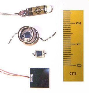
A photodiode is a semiconductor device that converts light into an electrical current. The current is generated when photons are absorbed in the photodiode. Photodiodes may contain optical filters, built-in lenses, and may have large or small surface areas. Photodiodes usually have a slower response time as their surface area increases. The common, traditional solar cell used to generate electric solar power is a large area photodiode.
Transistor–transistor logic (TTL) is a logic family built from bipolar junction transistors. Its name signifies that transistors perform both the logic function and the amplifying function ; it is the same naming convention used in resistor–transistor logic (RTL) and diode–transistor logic (DTL).

In electronics, a multi-transistor configuration called darlington pair, or the Darlington configuration is a compound structure of a particular design made by two bipolar transistors connected in such a way that the current amplified by the first transistor is amplified further by the second one. This configuration gives a much higher current gain than each transistor taken separately.

A p–n junction is a boundary or interface between two types of semiconductor materials, p-type and n-type, inside a single crystal of semiconductor. The "p" (positive) side contains an excess of holes, while the "n" (negative) side contains an excess of electrons in the outer shells of the electrically neutral atoms there. This allows electrical current to pass through the junction only in one direction. The p-n junction is created by doping, for example by ion implantation, diffusion of dopants, or by epitaxy. If two separate pieces of material were used, this would introduce a grain boundary between the semiconductors that would severely inhibit its utility by scattering the electrons and holes.

An electronic symbol is a pictogram used to represent various electrical and electronic devices or functions, such as wires, batteries, resistors, and transistors, in a schematic diagram of an electrical or electronic circuit. These symbols are largely standardized internationally today, but may vary from country to country, or engineering discipline, based on traditional conventions.

The point-contact transistor was the first type of transistor to be successfully demonstrated. It was developed by research scientists John Bardeen and Walter Brattain at Bell Laboratories in December 1947. They worked in a group led by physicist William Shockley. The group had been working together on experiments and theories of electric field effects in solid state materials, with the aim of replacing vacuum tubes with a smaller device that consumed less power.

Biasing in electronics means establishing predetermined voltages or currents at various points of an electronic circuit for the purpose of establishing proper operating conditions in electronic components.
A tetrode transistor is any transistor having four active terminals.
A diffused junction transistor is a transistor formed by diffusing dopants into a semiconductor substrate. The diffusion process was developed later than the alloy junction and grown junction processes for making BJTs.
A transistor is a semiconductor device with at least three terminals for connection to an electric circuit. The vacuum-tube triode, also called a (thermionic) valve, was the transistor's precursor, introduced in 1907. The principle of a field-effect transistor was proposed by Julius Edgar Lilienfeld in 1925.

Mohamed Mohamed Atalla was an Egyptian-American engineer, physical chemist, cryptographer, inventor and entrepreneur. His pioneering work in semiconductor technology laid the foundations for modern electronics. Most importantly, his invention of the MOSFET in 1959, along with his earlier surface passivation and thermal oxidation processes, revolutionized the electronics industry. He is also known as the founder of the data security company Atalla Corporation, founded in 1972, which introduced the first hardware security module and was a pioneer in online security. He received the Stuart Ballantine Medal and was inducted into the National Inventors Hall of Fame for his important contributions to semiconductor technology as well as data security.

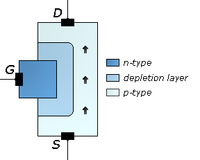
The field-effect transistor (FET) is an electronic device which uses an electric field to control the flow of current. FETs are devices with three terminals: source, gate, and drain. FETs control the flow of current by the application of a voltage to the gate, which in turn alters the conductivity between the drain and source.

