External links
- IPC Designers Council, Designer Certification – WAGO PCB Interconnect connector 2059 series Click
| | This computer-engineering-related article is a stub. You can help Wikipedia by expanding it. |
Certified Interconnect Designer (CID) is a certification from the IPC Designer's Council for experienced PCB design professionals. CID+ is the advanced version of this certification.
| | This computer-engineering-related article is a stub. You can help Wikipedia by expanding it. |
CID may refer to:

A printed circuit board is a medium used to connect electronic components to one another in a controlled manner. It takes the form of a laminated sandwich structure of conductive and insulating layers: each of the conductive layers is designed with an artwork pattern of traces, planes and other features etched from one or more sheet layers of copper laminated onto and/or between sheet layers of a non-conductive substrate. Electrical components may be fixed to conductive pads on the outer layers in the shape designed to accept the component's terminals, generally by means of soldering, to both electrically connect and mechanically fasten them to it. Another manufacturing process adds vias: plated-through holes that allow interconnections between layers.

Surface-mount technology (SMT), originally called planar mounting, is a method in which the electrical components are mounted directly onto the surface of a printed circuit board (PCB). An electrical component mounted in this manner is referred to as a surface-mount device (SMD). In industry, this approach has largely replaced the through-hole technology construction method of fitting components, in large part because SMT allows for increased manufacturing automation which reduces cost and improves quality. It also allows for more components to fit on a given area of substrate. Both technologies can be used on the same board, with the through-hole technology often used for components not suitable for surface mounting such as large transformers and heat-sinked power semiconductors.

The Gerber format is an open, ASCII, vector format for printed circuit board (PCB) designs. It is the de facto standard used by PCB industry software to describe the printed circuit board images: copper layers, solder mask, legend, drill data, etc.
The Pakistan Cricket Board (PCB) is a sports governing body for cricket in Pakistan responsible for controlling and organising all tours and matches undertaken by the Pakistan national cricket team. A member of the International Cricket Council since 1952, it represents the country's men's and women's national teams in international cricket tournaments played under the ICC.

TARGET 3001! is a CAD computer program for EDA and PCB design, developed by Ing.-Büro Friedrich in Germany. It supports the design of electronic schematics, PCBs, and device front panels. It runs under Windows and is available in English, German and French.
PCB NC drill files convey PCB drilling and routing information. The NC formats were originally designed by CNC drill and route machine vendors as proprietary input formats for their equipment, and are known under their company name: Excellon, Hitachi, Sieb & Meyer, Posalux, etc. These formats are similar as they are based on RS-274-C and related to G-code. In 1985 IPC published a generic standard NC format, IPC-NC-349. Later XNC was designed, a simple strict subset of IPC-NC-349, designed not for driving machines but for exchanging drill information between CAD and CAM. They are collectively referred to as (PCB) NC files.
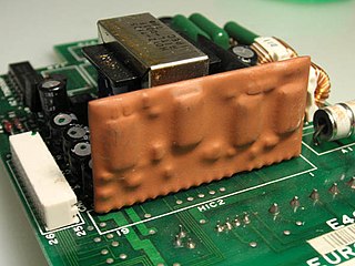
A hybrid integrated circuit (HIC), hybrid microcircuit, hybrid circuit or simply hybrid is a miniaturized electronic circuit constructed of individual devices, such as semiconductor devices and passive components, bonded to a substrate or printed circuit board (PCB). A PCB having components on a Printed Wiring Board (PWB) is not considered a true hybrid circuit according to the definition of MIL-PRF-38534.

Signal integrity or SI is a set of measures of the quality of an electrical signal. In digital electronics, a stream of binary values is represented by a voltage waveform. However, digital signals are fundamentally analog in nature, and all signals are subject to effects such as noise, distortion, and loss. Over short distances and at low bit rates, a simple conductor can transmit this with sufficient fidelity. At high bit rates and over longer distances or through various mediums, various effects can degrade the electrical signal to the point where errors occur and the system or device fails. Signal integrity engineering is the task of analyzing and mitigating these effects. It is an important activity at all levels of electronics packaging and assembly, from internal connections of an integrated circuit (IC), through the package, the printed circuit board (PCB), the backplane, and inter-system connections. While there are some common themes at these various levels, there are also practical considerations, in particular the interconnect flight time versus the bit period, that cause substantial differences in the approach to signal integrity for on-chip connections versus chip-to-chip connections.

Flat no-leads packages such as quad-flat no-leads (QFN) and dual-flat no-leads (DFN) physically and electrically connect integrated circuits to printed circuit boards. Flat no-leads, also known as micro leadframe (MLF) and SON, is a surface-mount technology, one of several package technologies that connect ICs to the surfaces of PCBs without through-holes. Flat no-lead is a near chip scale plastic encapsulated package made with a planar copper lead frame substrate. Perimeter lands on the package bottom provide electrical connections to the PCB. Flat no-lead packages usually, but not always, include an exposed thermally conductive pad to improve heat transfer out of the IC. Heat transfer can be further facilitated by metal vias in the thermal pad. The QFN package is similar to the quad-flat package (QFP), and a ball grid array (BGA).
A Fuzz Button is a high performance electrical connection material used to connect two parts of an electrical circuit together, for example an IC to a PCB or two PCBs to each other. Fuzz Buttons consist of a single strand of gold-plated beryllium copper wire compressed into a dense, sponge-like cylindrical shape. Their diameter can range from a few tenths of a millimetre to a millimetre.
IPC is a trade association whose aim is to standardize the assembly and production requirements of electronic equipment and assemblies. It was founded in 1957 as the Institute of Printed Circuits. Its name was later changed to the Institute for Interconnecting and Packaging Electronic Circuits to highlight the expansion from bare boards to packaging and electronic assemblies. In 1999, the organization formally changed its name to IPC with the accompanying tagline, Association Connecting Electronics Industries.
Microvias are used as the interconnects between layers in high density interconnect (HDI) substrates and printed circuit boards (PCBs) to accommodate the high input/output (I/O) density of advanced packages. Driven by portability and wireless communications, the electronics industry strives to produce affordable, light, and reliable products with increased functionality. At the electronic component level, this translates to components with increased I/Os with smaller footprint areas, and on the printed circuit board and package substrate level, to the use of high density interconnects (HDIs).
Altium Designer (AD) is a PCB and electronic design automation software package for printed circuit boards. It is developed by Australian software company Altium Limited.
Pad cratering is a mechanically induced fracture in the resin between copper foil and outermost layer of fiberglass of a printed circuit board (PCB). It may be within the resin or at the resin to fiberglass interface.
ODB++ is a proprietary CAD-to-CAM data exchange format used in the design and manufacture of electronic devices. Its purpose is to exchange printed circuit board design information between design and manufacturing and between design tools from different EDA/ECAD vendors. It was originally developed by Valor Computerized Systems, Ltd. as the job description format for their CAM system.
Schindler&Schill GmbH is a German software company, founded 2008 in Regensburg by two experts on Windows based software. The company also trades under EasyLogix.

The book-to-bill ratio, also known as the BB ratio or BO/BI ratio, is the ratio of orders received to the amount billed for a specific period, usually one month or one quarter. It is widely used in the technology sector and especially in the semiconductor industry, where the semiconductor manufacturing equipment (SME) book-to-bill ratio is considered an important leading indicator of demand trends.
Dye-n-Pry, also called Dye And Pry, Dye and Pull, Dye Staining, or Dye Penetrant, is a destructive analysis technique used on surface mount technology (SMT) components to either perform failure analysis or inspect for solder joint integrity. It is an application of dye penetrant inspection.
Conductive anodic filament, also called CAF, is a metallic filament that forms from an electrochemical migration process and is known to cause printed circuit board (PCB) failures.