Related Research Articles
The AMD Accelerated Processing Unit (APU), formerly known as Fusion, is the marketing term for a series of 64-bit microprocessors from Advanced Micro Devices (AMD), designed to act as a central processing unit (CPU) and graphics processing unit (GPU) on a single die. APUs are general purpose processors that feature integrated graphics processors (IGPs).

Haswell is the codename for a processor microarchitecture developed by Intel as the "fourth-generation core" successor to the Ivy Bridge. Intel officially announced CPUs based on this microarchitecture on June 4, 2013, at Computex Taipei 2013, while a working Haswell chip was demonstrated at the 2011 Intel Developer Forum. With Haswell, which uses a 22 nm process, Intel also introduced low-power processors designed for convertible or "hybrid" ultrabooks, designated by the "U" suffix.
Intel Core is a line of streamlined midrange consumer, workstation and enthusiast computer central processing units (CPUs) marketed by Intel Corporation. These processors displaced the existing mid- to high-end Pentium processors at the time of their introduction, moving the Pentium to the entry level. Identical or more capable versions of Core processors are also sold as Xeon processors for the server and workstation markets.

Intel Graphics Technology (GT) is the collective name for a series of integrated graphics processors (IGPs) produced by Intel that are manufactured on the same package or die as the central processing unit (CPU). It was first introduced in 2010 as Intel HD Graphics and renamed in 2017 as Intel UHD Graphics.

Skylake is the codename used by Intel for a processor microarchitecture that was launched in August 2015 succeeding the Broadwell microarchitecture. Skylake is a microarchitecture redesign using the same 14 nm manufacturing process technology as its predecessor, serving as a tock in Intel's tick–tock manufacturing and design model. According to Intel, the redesign brings greater CPU and GPU performance and reduced power consumption. Skylake CPUs share their microarchitecture with Kaby Lake, Coffee Lake, Cannon Lake, Whiskey Lake, and Comet Lake CPUs.

Broadwell is the fifth generation of the Intel Core Processor. It is Intel's codename for the 14 nanometer die shrink of its Haswell microarchitecture. It is a "tick" in Intel's tick–tock principle as the next step in semiconductor fabrication. Like some of the previous tick-tock iterations, Broadwell did not completely replace the full range of CPUs from the previous microarchitecture (Haswell), as there were no low-end desktop CPUs based on Broadwell.

LGA 1151, also known as Socket H4, is an Intel microprocessor compatible socket which comes in two distinct versions: the first revision which supports both Intel's Skylake and Kaby Lake CPUs, and the second revision which supports Coffee Lake CPUs exclusively.
Kaby Lake is Intel's codename for its seventh generation Core microprocessor family announced on August 30, 2016. Like the preceding Skylake, Kaby Lake is produced using a 14 nanometer manufacturing process technology. Breaking with Intel's previous "tick–tock" manufacturing and design model, Kaby Lake represents the optimized step of the newer process–architecture–optimization model. Kaby Lake began shipping to manufacturers and OEMs in the second quarter of 2016, and mobile chips have started shipping while Kaby Lake (desktop) chips were officially launched in January 2017.
Ice Lake is Intel's codename for the 10th generation Intel Core mobile and 3rd generation Xeon Scalable server processors based on the Sunny Cove microarchitecture. Ice Lake represents an Architecture step in Intel's Process-Architecture-Optimization model. Produced on the second generation of Intel's 10 nm process, 10 nm+, Ice Lake is Intel's second microarchitecture to be manufactured on the 10 nm process, following the limited launch of Cannon Lake in 2018. However, Intel altered their naming scheme in 2020 for the 10 nm process. In this new naming scheme, Ice Lake's manufacturing process is called simply 10 nm, without any appended pluses.
Tiger Lake is Intel's codename for the 11th generation Intel Core mobile processors based on the new Willow Cove Core microarchitecture, manufactured using Intel's third-generation 10 nm process node known as 10SF. Tiger Lake replaces the Ice Lake family of mobile processors, representing an Optimization step in Intel's process–architecture–optimization model.
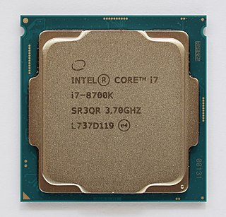
Coffee Lake is Intel's codename for its eighth generation Core microprocessor family, announced on September 25, 2017. It is manufactured using Intel's second 14 nm process node refinement. Desktop Coffee Lake processors introduced i5 and i7 CPUs featuring six cores and Core i3 CPUs with four cores and no hyperthreading.
Ryzen is a brand of multi-core x86-64 microprocessors designed and marketed by Advanced Micro Devices (AMD) for desktop, mobile, server, and embedded platforms based on the Zen microarchitecture. It consists of central processing units (CPUs) marketed for mainstream, enthusiast, server, and workstation segments and accelerated processing units (APUs) marketed for mainstream and entry-level segments and embedded systems applications.
Sapphire Rapids is a codename for Intel's fourth generation Xeon server processors based on Intel 7, which is a rebranded 10 nm Enhanced SuperFin process. Sapphire Rapids CPUs are designed for data centers; the roughly contemporary Alder Lake is intended for the wider public.
Cascade Lake is an Intel codename for a 14 nm server, workstation and enthusiast processor microarchitecture, launched in April 2019. In Intel's Process-Architecture-Optimization model, Cascade Lake is an optimization of Skylake. Intel states that this will be their first microarchitecture to support 3D XPoint-based memory modules. It also features Deep Learning Boost instructions and mitigations for Meltdown and Spectre. Intel officially launched new Xeon Scalable SKUs on February 24, 2020.
Process–architecture–optimization is a development model for central processing units (CPUs) that Intel adopted in 2016. Under this three-phase (three-year) model, every microprocessor die shrink is followed by a microarchitecture change and then by one or more optimizations. It replaced the two-phase (two-year) tick–tock model that Intel adopted in 2006. The tick–tock model was no longer economically sustainable, according to Intel, because production of ever smaller dies becomes ever more costly.

The ThinkPad P series line of laptops is produced by Lenovo and was introduced by the company as a successor to the previous ThinkPad W series. With 15.6" and 17.3" screens, the ThinkPad P series saw the reintroduction of physically large laptops into the ThinkPad line. Marketed largely as portable workstations, many P series laptops can be configured with high-end quad-core, hexa-core or octo-core Intel processors as well as ECC memory and a discrete Nvidia Quadro GPU. The P series offers ISV certifications from software vendors such as Adobe and Autodesk for various CAD software. The P52 and P72 models are the last current Lenovo laptops with a dedicated magnesium structural frame.

Intel Xe, earlier known unofficially as Gen12, is a GPU architecture developed by Intel.
Rocket Lake is Intel's codename for its 11th generation Core microprocessors. Released on March 30, 2021, it is based on the new Cypress Cove microarchitecture, a variant of Sunny Cove backported to Intel's 14 nm process node. Rocket Lake cores contain significantly more transistors than Skylake-derived Comet Lake cores.
Gracemont is a microarchitecture for low-power processors used in systems on a chip (SoCs) made by Intel, and is the successor to Tremont. Like its predecessor, it is also implemented as low-power cores in a hybrid design of the Alder Lake and Raptor Lake processors.
References
- "Products formerly Coffee Lake". ark.intel.com. Intel. Retrieved 20 December 2019.
- Cutress, Ian (12 July 2018). "Intel Launches Coffee Lake Xeon E (Entry): The Next-Gen E3-1200". AnandTech. Retrieved 18 December 2019.
- Cutress, Ian (4 November 2019). "Intel Launches Xeon-E 2200 Series for Servers: 8 Cores, up to 5.0 GHz". AnandTech. Retrieved 20 December 2019.
- Cutress, Ian (5 November 2018). "Intel Xeon E Six-Core Review: E-2186G, E-2176G, E-2146G, and E-2136 Tested". AnandTech. Retrieved 20 December 2019.
- Rißka, Volker (28 May 2019). "Intel-Prozessoren: 15 neue 9th Gen Core vPro und 14 Xeon E vorgestellt". ComputerBase (in German). Retrieved 20 December 2019.
- "Intel ufficializza gli Xeon E-2200 per il settore consumer". Tom's Hardware (in Italian).