
Ion implantation is a low-temperature process by which ions of one element are accelerated into a solid target, thereby changing the physical, chemical, or electrical properties of the target. Ion implantation is used in semiconductor device fabrication and in metal finishing, as well as in materials science research. The ions can alter the elemental composition of the target if they stop and remain in the target. Ion implantation also causes chemical and physical changes when the ions impinge on the target at high energy. The crystal structure of the target can be damaged or even destroyed by the energetic collision cascades, and ions of sufficiently high energy can cause nuclear transmutation.

MEMS is the technology of microscopic devices incorporating both electronic and moving parts. MEMS are made up of components between 1 and 100 micrometres in size, and MEMS devices generally range in size from 20 micrometres to a millimetre, although components arranged in arrays can be more than 1000 mm2. They usually consist of a central unit that processes data and several components that interact with the surroundings.

Semiconductor device fabrication is the process used to manufacture semiconductor devices, typically integrated circuits (ICs) such as computer processors, microcontrollers, and memory chips. It is a multiple-step photolithographic and physio-chemical process during which electronic circuits are gradually created on a wafer, typically made of pure single-crystal semiconducting material. Silicon is almost always used, but various compound semiconductors are used for specialized applications.
A semiconductor is a material that has an electrical conductivity value falling between that of a conductor, such as copper, and an insulator, such as glass. Its resistivity generally falls as its temperature rises; metals behave in the opposite way. In many cases their conducting properties may be altered in useful ways by introducing impurities ("doping") into the crystal structure. When two differently doped regions exist in the same crystal, a semiconductor junction is created. The behavior of charge carriers, which include electrons, ions, and electron holes, at these junctions is the basis of diodes, transistors, and most modern electronics. Some examples of semiconductors are silicon, germanium, gallium arsenide, and elements near the so-called "metalloid staircase" on the periodic table. After silicon, gallium arsenide is the second-most common semiconductor and is used in laser diodes, solar cells, microwave-frequency integrated circuits, and others. Silicon is a critical element for fabricating most electronic circuits.

Epitaxy refers to a type of crystal growth or material deposition in which new crystalline layers are formed with one or more well-defined orientations with respect to the crystalline seed layer. The deposited crystalline film is called an epitaxial film or epitaxial layer. The relative orientation(s) of the epitaxial layer to the seed layer is defined in terms of the orientation of the crystal lattice of each material. For most epitaxial growths, the new layer is usually crystalline and each crystallographic domain of the overlayer must have a well-defined orientation relative to the substrate crystal structure. Epitaxy can involve single-crystal structures, although grain-to-grain epitaxy has been observed in granular films. For most technological applications, single-domain epitaxy, which is the growth of an overlayer crystal with one well-defined orientation with respect to the substrate crystal, is preferred. Epitaxy can also play an important role while growing superlattice structures.
In semiconductor manufacturing, silicon on insulator (SOI) technology is fabrication of silicon semiconductor devices in a layered silicon–insulator–silicon substrate, to reduce parasitic capacitance within the device, thereby improving performance. SOI-based devices differ from conventional silicon-built devices in that the silicon junction is above an electrical insulator, typically silicon dioxide or sapphire. The choice of insulator depends largely on intended application, with sapphire being used for high-performance radio frequency (RF) and radiation-sensitive applications, and silicon dioxide for diminished short-channel effects in other microelectronics devices. The insulating layer and topmost silicon layer also vary widely with application.

In semiconductor production, doping is the intentional introduction of impurities into an intrinsic (undoped) semiconductor for the purpose of modulating its electrical, optical and structural properties. The doped material is referred to as an extrinsic semiconductor.
Rapid thermal processing (RTP) is a semiconductor manufacturing process which heats silicon wafers to temperatures exceeding 1,000°C for not more than a few seconds. During cooling wafer temperatures must be brought down slowly to prevent dislocations and wafer breakage due to thermal shock. Such rapid heating rates are often attained by high intensity lamps or lasers. These processes are used for a wide variety of applications in semiconductor manufacturing including dopant activation, thermal oxidation, metal reflow and chemical vapor deposition.
In metallurgy and materials science, annealing is a heat treatment that alters the physical and sometimes chemical properties of a material to increase its ductility and reduce its hardness, making it more workable. It involves heating a material above its recrystallization temperature, maintaining a suitable temperature for an appropriate amount of time and then cooling.

In microfabrication, thermal oxidation is a way to produce a thin layer of oxide on the surface of a wafer. The technique forces an oxidizing agent to diffuse into the wafer at high temperature and react with it. The rate of oxide growth is often predicted by the Deal–Grove model. Thermal oxidation may be applied to different materials, but most commonly involves the oxidation of silicon substrates to produce silicon dioxide.
Ion beam mixing is the atomic intermixing and alloying that can occur at the interface separating two different materials during ion irradiation. It is applied as a process for adhering two multilayers, especially a substrate and deposited surface layer. The process involves bombarding layered samples with doses of ion radiation in order to promote mixing at the interface, and generally serves as a means of preparing electrical junctions, especially between non-equilibrium or metastable alloys and intermetallic compounds. Ion implantation equipment can be used to achieve ion beam mixing.

A metal gate, in the context of a lateral metal–oxide–semiconductor (MOS) stack, is the gate electrode separated by an oxide from the transistor's channel – the gate material is made from a metal. In most MOS transistors since about the mid-1970s, the "M" for metal has been replaced by polysilicon, but the name remained.

Plasma-immersion ion implantation (PIII) or pulsed-plasma doping is a surface modification technique of extracting the accelerated ions from the plasma by applying a high voltage pulsed DC or pure DC power supply and targeting them into a suitable substrate or electrode with a semiconductor wafer placed over it, so as to implant it with suitable dopants. The electrode is a cathode for an electropositive plasma, while it is an anode for an electronegative plasma. Plasma can be generated in a suitably designed vacuum chamber with the help of various plasma sources such as electron cyclotron resonance plasma source which yields plasma with the highest ion density and lowest contamination level, helicon plasma source, capacitively coupled plasma source, inductively coupled plasma source, DC glow discharge and metal vapor arc. The vacuum chamber can be of two types - diode and triode type depending upon whether the power supply is applied to the substrate as in the former case or to the perforated grid as in the latter.
ASM is a Dutch headquartered multinational corporation that specializes in the design, manufacturing, sales and service of semiconductor wafer processing equipment for the fabrication of semiconductor devices. ASM's products are used by semiconductor manufacturers in front-end wafer processing in their semiconductor fabrication plants. ASM's technologies include atomic layer deposition, epitaxy, chemical vapor deposition and diffusion.
A dopant is a small amount of a substance added to a material to alter its physical properties, such as electrical or optical properties. The amount of dopant is typically very low compared to the material being doped.
Monolayer doping (MLD) in semiconductor production is a well controlled, wafer-scale surface doping technique first developed at the University of California, Berkeley, in 2007. This work is aimed for attaining controlled doping of semiconductor materials with atomic accuracy, especially at nanoscale, which is not easily obtained by other existing technologies. This technique is currently used for fabricating ultrashallow junctions (USJs) as the heavily doped source/drain (S/D) contacts of metal–oxide–semiconductor field effect transistors (MOSFETs) as well as enabling dopant profiling of nanostructures.
Ultra-high-purity steam, also called the clean steam, UHP steam or high purity water vapor, is used in a variety of industrial manufacturing processes that require oxidation or annealing. These processes include the growth of oxide layers on silicon wafers for the semiconductor industry, originally described by the Deal-Grove model, and for the formation of passivation layers used to improve the light capture ability of crystalline photovoltaic cells. Several methods and technologies can be employed to generate ultra high purity steam, including pyrolysis, bubbling, direct liquid injection, and purified steam generation. The level of purity, or the relative lack of contamination, affects the quality of the oxide layer or annealed surface. The method of delivery affects growth rate, uniformity, and electrical performance. Oxidation and annealing are common steps in the manufacture of such devices as microelectronics and solar cells.
Dopant activation is the process of obtaining the desired electronic contribution from impurity species in a semiconductor host. The term is often restricted to the application of thermal energy following the ion implantation of dopants. In the most common industrial example, rapid thermal processing is applied to silicon following the ion implantation of dopants such as phosphorus, arsenic and boron. Vacancies generated at elevated temperature (1200 °C) facilitate the movement of these species from interstitial to substitutional lattice sites while amorphization damage from the implantation process recrystallizes. A relatively rapid process, peak temperature is often maintained for less than one second to minimize unwanted chemical diffusion.
James W. Mayer was an applied physicist, who was active in the field of ion-solid interactions. His accomplishments played a critical role in the development of the solid-state particle detector; the field of ion beam analysis of materials, and the application of ion implantation to semiconductors.
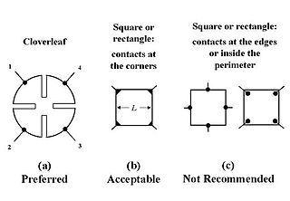
Differential Hall Effect Metrology (DHEM) measures all critical electrical parameters through an electrically active material at sub-nanometer depth resolution. DHEM is based on the previously developed Differential Hall Effect (DHE) method. In the traditional DHE method, successive sheet resistance and Hall effect measurements on a semiconductor layer are made using Van der Pauw and Hall effect techniques. The thickness of the layer is reduced through successive processing steps in between measurements. This typically involves thermal, chemical or electrochemical etching or oxidation to remove material from the measurement circuit. This data can be used to determine the depth profiles of carrier concentration, resistivity and mobility. DHE is a manual laboratory technique requiring wet chemical processing for etching and cleaning the sample between each measurement, and it has not been widely used in the semiconductor industry. Since the contact region is also affected by the material removal process, the traditional DHE approach requires that contacts be newly and repeatedly be made to collect data on the coupon. This introduces contact related noise and reduces the repeatability and stability of the data. The speed, accuracy and, depth resolution of DHE has been generally limited because of its manual nature. The DHEM technique is an improvement over the traditional DHE method in terms of automation, speed, data stability and, resolution. DHEM technique had been deployed in a semi-automated or automated tools.