Contents
- "Rocket Lake-S" (14 nm)
- Xeon W-13xx (workstation, uniprocessor)
- Xeon E-23xx (server, uniprocessor)
- References
The topic of this article may not meet Wikipedia's notability guideline for stand-alone lists .(May 2021) |
The topic of this article may not meet Wikipedia's notability guideline for stand-alone lists .(May 2021) |
| Model number | sSpec number | Cores (threads) | Frequency | Turbo | L2 cache | L3 cache | GPU model | GPU frequency | TDP | Socket | I/O bus | Release date | Part number(s) | Release price (USD) | ||
|---|---|---|---|---|---|---|---|---|---|---|---|---|---|---|---|---|
| Standard power | ||||||||||||||||
| Xeon W-1350 |
| 6 (12) | 3.3 GHz | 5.0 GHz | 6 × 512 KB | 12 MB | UHD Graphics P750 | 350-1300 MHz | 80 W | LGA 1200 | DMI 3.0 ×8 | May 2021 |
| $255 | ||
| Xeon W-1370 |
| 8 (16) | 2.9 GHz | 5.1 GHz | 8 × 512 KB | 16 MB | UHD Graphics P750 | 350-1300 MHz | 80 W | LGA 1200 | DMI 3.0 ×8 | May 2021 |
| $362 | ||
| Xeon W-1390 |
| 8 (16) | 2.8 GHz | 5.1 GHz (5.2 w/ TVB) | 8 × 512 KB | 16 MB | UHD Graphics P750 | 350-1300 MHz | 80 W | LGA 1200 | DMI 3.0 ×8 | May 2021 |
| $494 | ||
| High power | ||||||||||||||||
| Xeon W-1350P |
| 6 (12) | 4 GHz | 5.1 GHz | 6 × 512 KB | 12 MB | UHD Graphics P750 | 350-1300 MHz | 125 W | LGA 1200 | DMI 3.0 ×8 | May 2021 |
| $311 | ||
| Xeon W-1370P |
| 8 (16) | 3.6 GHz | 5.2 GHz | 8 × 512 KB | 16 MB | UHD Graphics P750 | 350-1300 MHz | 125 W | LGA 1200 | DMI 3.0 ×8 | May 2021 |
| $428 | ||
| Xeon W-1390P |
| 8 (16) | 3.5 GHz | 5.2 GHz (5.3 w/ TVB) | 8 × 512 KB | 16 MB | UHD Graphics P750 | 350-1300 MHz | 125 W | LGA 1200 | DMI 3.0 ×8 | May 2021 |
| $539 | ||
| Low power | ||||||||||||||||
| Xeon W-1390T |
| 8 (16) | 1.5 GHz | 4.9 GHz | 8 × 512 KB | 16 MB | UHD Graphics P750 | 350-1200 MHz | 35 W | LGA 1200 | DMI 3.0 ×8 | May 2021 |
| $494 | ||
| Model number | sSpec number | Cores (threads) | Frequency | Turbo | L2 cache | L3 cache | GPU model | GPU frequency | TDP | Socket | I/O bus | Release date | Part number(s) | Release price (USD) |
|---|---|---|---|---|---|---|---|---|---|---|---|---|---|---|
| Xeon E-2314 |
| 4 (4) | 2.8 GHz | 4.5 GHz | 4 × 512 KB | 8 MB | N/A | N/A | 65 W | LGA 1200 | DMI 3.0 ×8 | September 2021 |
| $182 |
| Xeon E-2324G |
| 4 (4) | 3.1 GHz | 4.6 GHz | 4 × 512 KB | 8 MB | UHD Graphics P750 | 350-1300 MHz | 65 W | LGA 1200 | DMI 3.0 ×8 | September 2021 |
| $209 $219 |
| Xeon E-2334 |
| 4 (8) | 3.4 GHz | 4.8 GHz | 4 × 512 KB | 8 MB | N/A | N/A | 65 W | LGA 1200 | DMI 3.0 ×8 | September 2021 |
| $250 $261 |
| Xeon E-2336 |
| 6 (12) | 2.9 GHz | 4.8 GHz | 6 × 512 KB | 12 MB | N/A | N/A | 65 W | LGA 1200 | DMI 3.0 ×8 | September 2021 |
| $284 $294 |
| Xeon E-2356G |
| 6 (12) | 3.2 GHz | 5.0 GHz | 6 × 512 KB | 12 MB | UHD Graphics P750 | 350-1300 MHz | 80 W | LGA 1200 | DMI 3.0 ×8 | September 2021 |
| $311 |
| Xeon E-2374G |
| 4 (8) | 3.7 GHz | 5.0 GHz | 4 × 512 KB | 8 MB | UHD Graphics P750 | 350-1300 MHz | 80 W | LGA 1200 | DMI 3.0 ×8 | September 2021 |
| $334 $345 |
| Xeon E-2378 |
| 8 (16) | 2.6 GHz | 4.8 GHz | 8 × 512 KB | 16 MB | N/A | N/A | 65 W | LGA 1200 | DMI 3.0 ×8 | September 2021 |
| $362 |
| Xeon E-2378G |
| 8 (16) | 2.8 GHz | 5.1 GHz | 8 × 512 KB | 16 MB | UHD Graphics P750 | 350-1300 MHz | 80 W | LGA 1200 | DMI 3.0 ×8 | September 2021 |
| $494 $505 |
| Xeon E-2386G |
| 6 (12) | 3.5 GHz | 5.1 GHz | 6 × 512 KB | 12 MB | UHD Graphics P750 | 350-1300 MHz | 95 W | LGA 1200 | DMI 3.0 ×8 | September 2021 |
| $450 |
| Xeon E-2388G |
| 8 (16) | 3.2 GHz | 5.1 GHz | 8 × 512 KB | 16 MB | UHD Graphics P750 | 350-1300 MHz | 95 W | LGA 1200 | DMI 3.0 ×8 | September 2021 |
| $539 |
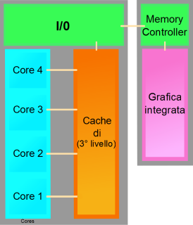
Xeon is a brand of x86 microprocessors designed, manufactured, and marketed by Intel, targeted at the non-consumer workstation, server, and embedded system markets. It was introduced in June 1998. Xeon processors are based on the same architecture as regular desktop-grade CPUs, but have advanced features such as support for ECC memory, higher core counts, more PCI Express lanes, support for larger amounts of RAM, larger cache memory and extra provision for enterprise-grade reliability, availability and serviceability (RAS) features responsible for handling hardware exceptions through the Machine Check Architecture. They are often capable of safely continuing execution where a normal processor cannot due to these extra RAS features, depending on the type and severity of the machine-check exception (MCE). Some also support multi-socket systems with two, four, or eight sockets through use of the Quick Path Interconnect (QPI) bus.
The AMD Accelerated Processing Unit (APU), formerly known as Fusion, is the marketing term for a series of 64-bit microprocessors from Advanced Micro Devices (AMD), designed to act as a central processing unit (CPU) and graphics processing unit (GPU) on a single die. APUs are general purpose processors that feature integrated graphics processors (IGPs).

Haswell is the codename for a processor microarchitecture developed by Intel as the "fourth-generation core" successor to the Ivy Bridge. Intel officially announced CPUs based on this microarchitecture on June 4, 2013, at Computex Taipei 2013, while a working Haswell chip was demonstrated at the 2011 Intel Developer Forum. With Haswell, which uses a 22 nm process, Intel also introduced low-power processors designed for convertible or "hybrid" ultrabooks, designated by the "U" suffix.

Skylake is the codename used by Intel for a processor microarchitecture that was launched in August 2015 succeeding the Broadwell microarchitecture. Skylake is a microarchitecture redesign using the same 14 nm manufacturing process technology as its predecessor, serving as a tock in Intel's tick–tock manufacturing and design model. According to Intel, the redesign brings greater CPU and GPU performance and reduced power consumption. Skylake CPUs share their microarchitecture with Kaby Lake, Coffee Lake, Cannon Lake, Whiskey Lake, and Comet Lake CPUs.

Ivy Bridge is the codename for Intel's 22 nm microarchitecture used in the third generation of the Intel Core processors. Ivy Bridge is a die shrink to 22 nm process based on FinFET ("3D") Tri-Gate transistors, from the former generation's 32 nm Sandy Bridge microarchitecture—also known as tick–tock model. The name is also applied more broadly to the Xeon and Core i7 Ivy Bridge-E series of processors released in 2013.
Westmere is the code name given to the 32 nm die shrink of Nehalem. While sharing the same CPU sockets, Westmere included Intel HD Graphics, while Nehalem did not.

Broadwell is the fifth generation of the Intel Core Processor. It is Intel's codename for the 14 nanometer die shrink of its Haswell microarchitecture. It is a "tick" in Intel's tick–tock principle as the next step in semiconductor fabrication. Like some of the previous tick-tock iterations, Broadwell did not completely replace the full range of CPUs from the previous microarchitecture (Haswell), as there were no low-end desktop CPUs based on Broadwell.
Kaby Lake is Intel's codename for its seventh generation Core microprocessor family announced on August 30, 2016. Like the preceding Skylake, Kaby Lake is produced using a 14 nanometer manufacturing process technology. Breaking with Intel's previous "tick–tock" manufacturing and design model, Kaby Lake represents the optimized step of the newer process–architecture–optimization model. Kaby Lake began shipping to manufacturers and OEMs in the second quarter of 2016, and mobile chips have started shipping while Kaby Lake (desktop) chips were officially launched in January 2017.
Ice Lake is Intel's codename for the 10th generation Intel Core mobile and 3rd generation Xeon Scalable server processors based on the Sunny Cove microarchitecture. Ice Lake represents an Architecture step in Intel's Process-Architecture-Optimization model. Produced on the second generation of Intel's 10 nm process, 10 nm+, Ice Lake is Intel's second microarchitecture to be manufactured on the 10 nm process, following the limited launch of Cannon Lake in 2018. However, Intel altered their naming scheme in 2020 for the 10 nm process. In this new naming scheme, Ice Lake's manufacturing process is called simply 10 nm, without any appended pluses.
Tiger Lake is Intel's codename for the 11th generation Intel Core mobile processors based on the new Willow Cove Core microarchitecture, manufactured using Intel's third-generation 10 nm process node known as 10SF. Tiger Lake replaces the Ice Lake family of mobile processors, representing an Optimization step in Intel's process–architecture–optimization model.

The ThinkPad P series line of laptops is produced by Lenovo and was introduced by the company as a successor to the previous ThinkPad W series. With 15.6" and 17.3" screens, the ThinkPad P series saw the reintroduction of physically large laptops into the ThinkPad line. Marketed largely as portable workstations, many P series laptops can be configured with high-end quad-core, hexa-core or octo-core Intel processors as well as ECC memory and a discrete Nvidia Quadro GPU. The P series offers ISV certifications from software vendors such as Adobe and Autodesk for various CAD software. The P52 and P72 models are the last current Lenovo laptops with a dedicated magnesium structural frame.

Intel Xe, earlier known unofficially as Gen12, is a GPU architecture developed by Intel.