Memory-mapped I/O and port-mapped I/O

Last updated

Memory-mapped I/O (MMIO) and port-mapped I/O (PMIO) are two complementary methods of performing input/output (I/O) between the central processing unit (CPU) and peripheral devices in a computer (often mediating access via chipset). An alternative approach is using dedicated I/O processors, commonly known as channels on mainframe computers, which execute their own instructions.

Contents

Memory-mapped I/O uses the same address space to address both main memory [lower-alpha 1] and I/O devices. [1] The memory and registers of the I/O devices are mapped to (associated with) address values, so a memory address may refer to either a portion of physical RAM or to memory and registers of the I/O device. Thus, the CPU instructions used to access the memory (e.g. MOV ...) can also be used for accessing devices. Each I/O device either monitors the CPU's address bus and responds to any CPU access of an address assigned to that device, connecting the system bus to the desired device's hardware register, or uses a dedicated bus.

To accommodate the I/O devices, some areas of the address bus used by the CPU must be reserved for I/O and must not be available for normal physical memory; the range of addresses used for I/O devices is determined by the hardware. The reservation may be permanent, or temporary (as achieved via bank switching). An example of the latter is found in the Commodore 64, which uses a form of memory mapping to cause RAM or I/O hardware to appear in the 0xD000-0xDFFF range.

Port-mapped I/O often uses a special class of CPU instructions designed specifically for performing I/O, such as the in and out instructions found on microprocessors based on the x86 architecture. Different forms of these two instructions can copy one, two or four bytes (outb, outw and outl, respectively) between the EAX register or one of that register's subdivisions on the CPU and a specified I/O port address which is assigned to an I/O device. I/O devices have a separate address space from general memory, either accomplished by an extra "I/O" pin on the CPU's physical interface, or an entire bus dedicated to I/O. Because the address space for I/O is isolated from that for main memory, this is sometimes referred to as isolated I/O. [2] On the x86 architecture, index/data pair is often used for port-mapped I/O. [3]

Overview

Different CPU-to-device communication methods, such as memory mapping, do not affect the direct memory access (DMA) for a device, because, by definition, DMA is a memory-to-device communication method that bypasses the CPU.

Hardware interrupts are another communication method between the CPU and peripheral devices, however, for a number of reasons, interrupts are always treated separately. An interrupt is device-initiated, as opposed to the methods mentioned above, which are CPU-initiated. It is also unidirectional, as information flows only from device to CPU. Lastly, each interrupt line carries only one bit of information with a fixed meaning, namely "an event that requires attention has occurred in a device on this interrupt line".

I/O operations can slow memory access if the address and data buses are shared. This is because the peripheral device is usually much slower than main memory. In some architectures, port-mapped I/O operates via a dedicated I/O bus, alleviating the problem.

One merit of memory-mapped I/O is that, by discarding the extra complexity that port I/O brings, a CPU requires less internal logic and is thus cheaper, faster, easier to build, consumes less power and can be physically smaller; this follows the basic tenets of reduced instruction set computing, and is also advantageous in embedded systems. The other advantage is that, because regular memory instructions are used to address devices, all of the CPU's addressing modes are available for the I/O as well as the memory, and instructions that perform an ALU operation directly on a memory operand (loading an operand from a memory location, storing the result to a memory location, or both) can be used with I/O device registers as well. In contrast, port-mapped I/O instructions are often very limited, often providing only for simple load-and-store operations between CPU registers and I/O ports, so that, for example, to add a constant to a port-mapped device register would require three instructions: read the port to a CPU register, add the constant to the CPU register, and write the result back to the port.

As 16-bit processors have become obsolete and replaced with 32-bit and 64-bit in general use, reserving ranges of memory address space for I/O is less of a problem, as the memory address space of the processor is usually much larger than the required space for all memory and I/O devices in a system. Therefore, it has become more frequently practical to take advantage of the benefits of memory-mapped I/O. However, even with address space being no longer a major concern, neither I/O mapping method is universally superior to the other, and there will be cases where using port-mapped I/O is still preferable.

x86

Memory-mapped I/O is preferred in x86-based architectures because the instructions that perform port-based I/O are limited to one register: EAX, AX, and AL are the only registers that data can be moved into or out of, and either a byte-sized immediate value in the instruction or a value in register DX determines which port is the source or destination port of the transfer. [4] [5] Since any general-purpose register can send or receive data to or from memory and memory-mapped I/O devices, memory-mapped I/O uses fewer instructions and can run faster than port I/O. AMD did not extend the port I/O instructions when defining the x86-64 architecture to support 64-bit ports, so 64-bit transfers cannot be performed using port I/O. [6]

On newer Intel platforms beginning with 2008 5 series, I/O devices on the chipset directly communicate via a dedicated Direct Media Interface (DMI) bus. [lower-alpha 2] [7]

Memory barriers

Since the caches mediate accesses to memory addresses, data written to different addresses may reach the peripherals' memory or registers out of the program order, i.e. if software writes data to an address and then writes data to another address, the cache write buffer does not guarantee that the data will reach the peripherals in that order. [8] Any program that does not include cache-flushing instructions after each write in the sequence may see unintended IO effects if a cache system optimizes the write order. Writes to memory can often be reordered to reduce redundancy or to make better use of memory access cycles without changing the final state of what got stored; whereas, the same optimizations might completely change the meaning and effect of writes to memory-mapped I/O regions.

Lack of foresight in the choice of memory-mapped I/O regions led to many of the RAM-capacity barriers in older generations of computers. Designers rarely expected machines to grow to make full use of an architecture's theoretical RAM capacity, and thus often used some of the high-order bits of the address-space as selectors for memory-mapped I/O functions. For example, the 640 KB barrier in the IBM PC and derivatives is due to reserving the region between 640 and 1024 KB (64k segments 10 through 16) for the Upper Memory Area. This choice initially made little impact, but it eventually limited the total amount of RAM available within the 20-bit available address space. The 3 GB barrier and PCI hole are similar manifestations of this with 32-bit address spaces, exacerbated by details of the x86 boot process and MMU design. 64-bit architectures often technically have similar issues, but these only rarely have practical consequences.

Examples

A sample system memory map
Address range (hexadecimal)SizeDevice
00007FFF32 KiBRAM
800080FF256 bytesGeneral-purpose I/O
900090FF256 bytesSound controller
A000A7FF2 KiBVideo controller/text-mapped display RAM
C000FFFF16 KiBROM

A simple system built around an 8-bit microprocessor might provide 16-bit address lines, allowing it to address up to 64  kibibytes (KiB) of memory. On such a system, the first 32 KiB of address space may be allotted to random access memory (RAM), another 16 KiB to read-only memory (ROM) and the remainder to a variety of other devices such as timers, counters, video display chips, sound generating devices, etc.

The hardware of the system is arranged so that devices on the address bus will only respond to particular addresses which are intended for them, while all other addresses are ignored. This is the job of the address decoding circuitry, and that establishes the memory map of the system. As a result, system's memory map may look like in the table on the right. This memory map contains gaps, which is also quite common in actual system architectures.

Assuming the fourth register of the video controller sets the background colour of the screen, the CPU can set this colour by writing a value to the memory location A003 using its standard memory write instruction. Using the same method, graphs can be displayed on a screen by writing character values into a special area of RAM within the video controller. Prior to cheap RAM that enabled bit-mapped displays, this character cell method was a popular technique for computer video displays (see Text user interface).

Basic types of address decoding

Address decoding types, in which a device may decode addresses completely or incompletely, include the following:

Complete (exhaustive) decoding
1:1 mapping of unique addresses to one hardware register (physical memory location). Involves checking every line of the address bus.
Incomplete (partial) decoding
n:1 mapping of n unique addresses to one hardware register. Partial decoding allows a memory location to have more than one address, allowing the programmer to reference a memory location using n different addresses. It may also be done to simplify the decoding hardware by using simpler and often cheaper logic that examines only some address lines, when not all of the CPU's address space is needed. Commonly, the decoding itself is programmable, so the system can reconfigure its own memory map as required, though this is a newer development and generally in conflict with the intent of being cheaper.
Synonyms: foldback, multiply mapped, partially mapped, address aliasing. [9] [10]
Linear decoding
Address lines are used directly without any decoding logic. This is done with devices such as RAMs and ROMs that have a sequence of address inputs, and with peripheral chips that have a similar sequence of inputs for addressing a bank of registers. Linear addressing is rarely used alone (only when there are few devices on the bus, as using purely linear addressing for more than one device usually wastes a lot of address space) but instead is combined with one of the other methods to select a device or group of devices within which the linear addressing selects a single register or memory location.

Port I/O via device drivers

In Windows-based computers, memory can also be accessed via specific drivers such as DOLLx8KD which gives I/O access in 8-, 16- and 32-bit on most Windows platforms starting from Windows 95 up to Windows 7. Installing I/O port drivers will ensure memory access by activating the drivers with simple DLL calls allowing port I/O and when not needed, the driver can be closed to prevent unauthorized access to the I/O ports.

Linux provides the pcimem utility to allow reading from and writing to MMIO addresses. The Linux kernel also allows tracing MMIO access from kernel modules (drivers) using the kernel's mmiotrace debug facility. To enable this, the Linux kernel should be compiled with the corresponding option enabled. mmiotrace is used for debugging closed-source device drivers.

See also

Notes

  1. A memory that besides registers is directly accessible by the processor, e.g. DRAM in IBM PC compatible computers or Flash/SRAM in microcontrollers.
  2. See Intel datasheets on specific CPU family e.g. 2014 "10th Generation Intel Processor Families" (PDF). Intel. April 2020. Retrieved 2023-06-05.;

Related Research Articles

<span class="mw-page-title-main">Intel 8080</span> 8-bit microprocessor

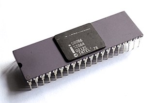
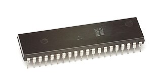
The Intel 8080 ("eighty-eighty") is the second 8-bit microprocessor designed and manufactured by Intel. It first appeared in April 1974 and is an extended and enhanced variant of the earlier 8008 design, although without binary compatibility. The initial specified clock rate or frequency limit was 2 MHz, with common instructions using 4, 5, 7, 10, or 11 cycles. As a result, the processor is able to execute several hundred thousand instructions per second. Two faster variants, the 8080A-1 and 8080A-2, became available later with clock frequency limits of 3.125 MHz and 2.63 MHz respectively. The 8080 needs two support chips to function in most applications: the i8224 clock generator/driver and the i8228 bus controller. It is implemented in N-type metal–oxide–semiconductor logic (NMOS) using non-saturated enhancement mode transistors as loads thus demanding a +12 V and a −5 V voltage in addition to the main transistor–transistor logic (TTL) compatible +5 V.

<span class="mw-page-title-main">Intel 8086</span> 16-bit microprocessor

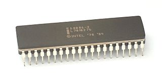
The 8086 is a 16-bit microprocessor chip designed by Intel between early 1976 and June 8, 1978, when it was released. The Intel 8088, released July 1, 1979, is a slightly modified chip with an external 8-bit data bus, and is notable as the processor used in the original IBM PC design.

x86 Family of instruction set architectures

x86 is a family of complex instruction set computer (CISC) instruction set architectures initially developed by Intel based on the Intel 8086 microprocessor and its 8088 variant. The 8086 was introduced in 1978 as a fully 16-bit extension of Intel's 8-bit 8080 microprocessor, with memory segmentation as a solution for addressing more memory than can be covered by a plain 16-bit address. The term "x86" came into being because the names of several successors to Intel's 8086 processor end in "86", including the 80186, 80286, 80386 and 80486 processors. Colloquially, their names were "186", "286", "386" and "486".

Direct memory access (DMA) is a feature of computer systems that allows certain hardware subsystems to access main system memory independently of the central processing unit (CPU).

<span class="mw-page-title-main">MCS-51</span> Single chip microcontroller series by Intel

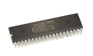
The Intel MCS-51 is a single chip microcontroller (MCU) series developed by Intel in 1980 for use in embedded systems. The architect of the Intel MCS-51 instruction set was John H. Wharton. Intel's original versions were popular in the 1980s and early 1990s, and enhanced binary compatible derivatives remain popular today. It is a complex instruction set computer, but also has some of the features of RISC architectures, such as a large register set and register windows, and has separate memory spaces for program instructions and data.

<span class="mw-page-title-main">Intel 8085</span> 8-bit microprocessor by Intel

The Intel 8085 ("eighty-eighty-five") is an 8-bit microprocessor produced by Intel and introduced in March 1976. It is the last 8-bit microprocessor developed by Intel.

<span class="mw-page-title-main">Intel 4040</span> 4-bit microprocessor introduced in 1974 by Intel

The Intel 4040 microprocessor was the successor to the Intel 4004, introduced in 1974. The 4040 employed a 10 μm silicon gate enhancement-load PMOS technology, was made up of 3,000 transistors and could execute approximately 62,000 instructions per second.

<span class="mw-page-title-main">64-bit computing</span> Computer architecture bit width

In computer architecture, 64-bit integers, memory addresses, or other data units are those that are 64 bits wide. Also, 64-bit central processing units (CPU) and arithmetic logic units (ALU) are those that are based on processor registers, address buses, or data buses of that size. A computer that uses such a processor is a 64-bit computer.

In computing, protected mode, also called protected virtual address mode, is an operational mode of x86-compatible central processing units (CPUs). It allows system software to use features such as segmentation, virtual memory, paging and safe multi-tasking designed to increase an operating system's control over application software.

<span class="mw-page-title-main">PIC microcontrollers</span> Line of single-chip microprocessors from Microchip Technology

PIC is a family of microcontrollers made by Microchip Technology, derived from the PIC1640 originally developed by General Instrument's Microelectronics Division. The name PIC initially referred to Peripheral Interface Controller, and is currently expanded as Programmable Intelligent Computer. The first parts of the family were available in 1976; by 2013 the company had shipped more than twelve billion individual parts, used in a wide variety of embedded systems.

<span class="mw-page-title-main">Bank switching</span> A technique to increase the amount of usable memory

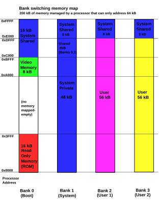
Bank switching is a technique used in computer design to increase the amount of usable memory beyond the amount directly addressable by the processor instructions. It can be used to configure a system differently at different times; for example, a ROM required to start a system from diskette could be switched out when no longer needed. In video game systems, bank switching allowed larger games to be developed for play on existing consoles.

<span class="mw-page-title-main">Zilog Z8000</span> 16-bit microprocessor

The Z8000 is a 16-bit microprocessor introduced by Zilog in early 1979. The architecture was designed by Bernard Peuto while the logic and physical implementation was done by Masatoshi Shima, assisted by a small group of people. In contrast to most designs of the era, the Z8000 did not use microcode which allowed it to be implemented in only 17,500 transistors.

PCI configuration space is the underlying way that the Conventional PCI, PCI-X and PCI Express perform auto configuration of the cards inserted into their bus.

<span class="mw-page-title-main">Blackfin</span> Family of 16-/32-bit microprocessors

The Blackfin is a family of 16-/32-bit microprocessors developed, manufactured and marketed by Analog Devices. The processors have built-in, fixed-point digital signal processor (DSP) functionality performed by 16-bit multiply–accumulates (MACs), accompanied on-chip by a microcontroller. It was designed for a unified low-power processor architecture that can run operating systems while simultaneously handling complex numeric tasks such as real-time H.264 video encoding.

<span class="mw-page-title-main">QEMU</span> Free virtualization and emulation software

QEMU is a free and open-source emulator. It emulates a computer's processor through dynamic binary translation and provides a set of different hardware and device models for the machine, enabling it to run a variety of guest operating systems. It can interoperate with Kernel-based Virtual Machine (KVM) to run virtual machines at near-native speed. QEMU can also do emulation for user-level processes, allowing applications compiled for one architecture to run on another.

<span class="mw-page-title-main">Signetics 2650</span> 8-bit microprocessor

The Signetics 2650 was an 8-bit microprocessor introduced in July 1975. According to Adam Osborne's book An Introduction to Microprocessors Vol 2: Some Real Products, it was "the most minicomputer-like" of the microprocessors available at the time. A combination of missing features and odd memory access limited its appeal, and the system saw little use in the market.

<span class="mw-page-title-main">Input–output memory management unit</span> Configuration in computing

In computing, an input–output memory management unit (IOMMU) is a memory management unit (MMU) connecting a direct-memory-access–capable (DMA-capable) I/O bus to the main memory. Like a traditional MMU, which translates CPU-visible virtual addresses to physical addresses, the IOMMU maps device-visible virtual addresses to physical addresses. Some units also provide memory protection from faulty or malicious devices.

The maximum random access memory (RAM) installed in any computer system is limited by hardware, software and economic factors. The hardware may have a limited number of address bus bits, limited by the processor package or design of the system. Some of the address space may be shared between RAM, peripherals, and read-only memory. In the case of a microcontroller with no external RAM, the size of the RAM array is limited by the size of the integrated circuit die. In a packaged system, only enough RAM may be provided for the system's required functions, with no provision for addition of memory after manufacture.

In computing, the term 3 GB barrier refers to a limitation of some 32-bit operating systems running on x86 microprocessors. It prevents the operating systems from using all of 4 GiB (4 × 10243 bytes) of main memory. The exact barrier varies by motherboard and I/O device configuration, particularly the size of video RAM; it may be in the range of 2.75 GB to 3.5 GB. The barrier is not present with a 64-bit processor and 64-bit operating system, or with certain x86 hardware and an operating system such as Linux or certain versions of Windows Server and macOS that allow use of Physical Address Extension (PAE) mode on x86 to access more than 4 GiB of RAM.

This glossary of computer hardware terms is a list of definitions of terms and concepts related to computer hardware, i.e. the physical and structural components of computers, architectural issues, and peripheral devices.

References

  1. Hayes, John P. (1978). Computer Architecture and Organization. McGraw-Hill International Book Company. p. 419. ISBN   0-07-027363-4.
  2. Dandamudi, Sivarama P. (2006-05-31). "Chapter 19 Input/Output Organization" (PDF). Fundamentals of Computer Organization and Design. Springer Science+Business Media. ISBN   978-0-387-21566-2.
  3. "Bochs VBE Extensions - OSDev Wiki".
  4. "Intel 64 and IA-32 Architectures Software Developer's Manual: Volume 2A: Instruction Set Reference, A-M" (PDF). Intel 64 and IA-32 Architectures Software Developer's Manual. Intel Corporation. June 2010. pp. 3–520. Retrieved 2010-08-21.
  5. "Intel 64 and IA-32 Architectures Software Developer's Manual: Volume 2B: Instruction Set Reference, N-Z" (PDF). Intel 64 and IA-32 Architectures Software Developer's Manual. Intel Corporation. June 2010. pp. 4–22. Retrieved 2010-08-21.
  6. "AMD64 Architecture Programmer's Manual: Volume 3: General-Purpose and System Instructions" (PDF). AMD64 Architecture Programmer's Manual. Advanced Micro Devices. November 2009. pp. 117, 181. Retrieved 2010-08-21.
  7. "What Is the Direct Media Interface (DMI) of Intel Processors?". Intel. Retrieved 2023-06-05.
  8. ARM Cortex-A Series Programmer's Guide. Literature number ARM DEN0013D. pp. 10–13.
  9. "Partial Address Decoding and I/O Space in Windows Operating Systems". Microsoft. 2001-12-04.
  10. "Address aliasing". Hewlett-Packard.