National Semiconductor SC/MP

Last updated
National Semiconductor SC/MP
National Semiconductor SCMP-die.jpg
PMOS SC/MP die (ISP-8A/500)
General information
LaunchedApril 1976;47 years ago (April 1976)
Common manufacturer(s)
Performance
Max. CPU clock rate 1 MHz to 4 MHz
Data width 8 bits
Address width 16 bits
Physical specifications
Package(s)

National Semiconductor's SC/MP (pronounced scamp) for Simple Cost-effective Micro Processor, is an early 8-bit microprocessor which became available in April 1976. It was designed to allow systems to be implemented with the minimum number of additional support chips. SC/MP included a daisy-chained control pin that allowed up to three SC/MP's share a single main memory to produce a multiprocessor system, or to act as controllers in a system with another main central processing unit (CPU). Three versions were released over its lifetime, SCMP-1 through 3, the latter two also known as INS8060 and INS8070.

Contents

To lower cost, the system used a bit-serial arithmetic logic unit (ALU) and was thus significantly slower than contemporary designs like the Intel 8080 or MOS 6502 which had parallel ALUs. Another oddity was that the program counter could only access the lower 12-bits of the 16-bit address, and the upper 4-bits had to be set using special instructions. The result was that instructions accessed main memory as sixteen 4 kB "pages" and reaching memory outside those pages required multiple instructions. [lower-alpha 1]

The combination of slow speed and paged memory limited its attractiveness outside the embedded markets it was aimed at, and in this market it competed against the Fairchild F8 which had a number of useful additional features. The system saw relatively little use.

Design

NS SC/MP registers
15. . .07. . .00(bit position)
Pointer registers
P0 (PC)Pointer 0 / Program Counter
P1Pointer 1
P2Pointer 2
P3Pointer 3
 ACAccumulator
 EExtension
Program Status Register
76543210(bit position)
CY OV SBSA IE F2F1F0Status

ALU and main registers

The arithmetic logic unit (ALU) was accumulator-based, with a single 8-bit accumulator, AC. A second 8-bit register, "Extension", or E, could be used as a backup for AC. E could not be accessed directly by most instructions, one could not load data from memory directly into E for instance. Instead, the value in AC could be written to or read from E, and another instruction swapped the two values in a single instruction. This allowed it to be used in a fashion similar to the mirror registers seen in designs like the Zilog Z80, with E acting as a quick way to store the value of AC during an interrupt. [1]

The main purpose of E was to act as a buffer for the built-in serial I/O system. [2] This was driven by the SIO instruction, which bit shifted the least significant bit in E to a latch which was connected to the SOUT pin on the processor. Repeated calls to SIO thus presented bits of the 8-bit E value one at a time to the output, or reversed this operation for reading from the SIN pin. [3] Once a complete 8-bit value had been read or written, the value could be sent to memory by exchanging the value with A and then loading or storing A to memory. [1] E could also be used as the source for logical operations on AC, so for instance, one could read a status byte in from the serial port and then AND that value with a mask in AC, to check for various status bits read from an external device. [4]

The separate Status Register was 8-bits. The three least-significant-bits, 0 through 2, were connected directly to pins, providing an easy way to check external device's status. [1] A further two pins, Sense A and B, were connected to bits 4 and 5. Sense A was normally used to service interrupts (see details below). Interrupts could be turned off by setting bit 3, Interrupt Enable (IE) to 0 with the Disable Interrupt instruction, DINT, and enabled with IEN, or by moving the value to and from A and manipulating it there. Bits 6 and 7 were conventional overflow and carry flags, as seen in most processors. [5]

Addressing and index registers

Like most 8-bit microprocessors of the era, the SC/MP is based around a 16-bit address and an 8-bit data bus. To lower pin count, the external address bus contains only 12 pins, sharing 4 pins from the data bus to create a complete 16-bit address. [2] Internally, the program counter is twelve bits wide, and there are separate instructions to set the upper four bits by copying an 8-bit value into the high byte. This provides a memory map of sixteen four-kilobyte pages, and program code could not refer to code or data outside its own page. [6] Thus the memory is arranged as 16 pages of 4 kB each. This leads to a curiosity of the design; when the program counter reaches the end of a page, it does not move to the next page, it returns to the start of the current page. [2]

This was further limited by the two-byte instruction format, which used one byte for the opcode and a second one to indicate an offset between -128 and +127, which was added to a value in the processor registers to produce a complete 16-bit address. For instance, an address might refer to a location in memory by saying it is +10 locations from the value in the program counter, or +10 from the value in one of the 16-bit index registers. To access a location outside that range, the address had to be stored in one of the index registers, and then the offset set to zero. [6] Because the registers are 16-bit, and the accumulator that loads values is 8-bit, setting a complete address required several instructions. [7]

As indexes were critical to the addressing model, the SC/MP included four index registers, the "Pointer Registers" PR0 through PR3. PR0 was the program counter, and not normally manipulated by user programs. By convention, PR1 was normally used as a pointer into ROM, PR2 into RAM, and PR3 was used to store an address during interrupts and subroutine calls. [5] The SC/MP did not have a stack, where return values were normally stored on most contemporary designs. Programs had to save return addresses with explicit code. [7]

There were four primary addressing modes, PC-relative, indexed, immediate (meaning a constant in the instruction's second byte as opposed to an offset), and auto-indexed. PC-relative addressing was actually the same as indexed, selecting PR0 as the index register. [6]

Auto-indexed is used to aid the construction of loops. If the displacement is less than zero, the contents of the Pointer Register is decreased by the displacement before the contents of the effective address are fetched or stored. If the displacement is equal to or greater than zero, the contents of the Pointer Register are used as the effective address, and the contents of the Pointer Register are increased by the displacement after the contents of the effective address are fetched or stored. This removes the need for a separate instruction to change the value in the register, so one could store the starting value of a block of data in memory in a PR and then loop through all of the data by calling a single instruction. [6] If the offset is negative it performs the decrement before accessing the final value, if it is positive, it does a post-increment. [7]

Interrupt handling

The system includes automatic handling of interrupts on the Sense A line. When an interrupt is received and IE is high (enabled), before starting to fetch the next instruction the system instead clears IE to prevent another interrupt, and then exchanges the values in PC and PS3. This has the effect of saving the return address in PR3 and sending the next instruction into the interrupt handler entry point previously stored in PR3. [8]

The system does not include the equivalent of a return-from-interrupt. This can be performed with another XPPC, copying the previously-saved address in PR3 back to the PC and execution continues where it left off. However, this leaves the wrong address in PR3, not the start of the interrupt handler, but the end. To address this, the common solution is to place the XPPC that returns to the main code one instruction above the handler entry point, rather than at the end. When the handler completes, it jumps back to this instruction, so when XPPC is called, the PC is pointed one location before the proper entry point. Because the system increments the PC before calling an instruction, this means the next interrupt will result it in entering at the correct entry point. This "exit handler" normally also resets the IE to 1 to re-enable interrupts. [9]

Bus control

National Semiconductor SC/MP Development System National Semiconductor SC-MP Development System.jpg
National Semiconductor SC/MP Development System

A feature of the SC/MP was a shared daisy-chained control line that allowed multiple SC/MP, or more commonly a single SC/MP and related direct memory access (DMA) controllers, to share access to a single main memory. When any one of the chips on the bus desired access to memory, it would set the ENOUT pin high, thereby signalling the other chip's ENIN pins that they had to release the bus. With most other processors, this would normally require external logic implemented by the board designers to pause the CPU to the same end, often with some complexity due to the internal instruction timing that was not visible to the external circuits. In the SC/MP this was all included internally so a single line on the circuit board was all that was needed to implement this feature. [10]

The original idea was to ease the creation of microcontroller-like applications containing an SC/MP, one or more DMA controllers, and a single shared memory. Designed specifically to be as low-cost as possible in terms of an overall system, the desire to lower the cost of the SC/MP itself also led to decisions about the bit-serial ALU and the inclusion of serial input/output lines to eliminate the need for a separate UART (this feature was removed in the later SC/MP III). [11] Osborne's review of the system stated it was the "microprocessor of choice in any multi-processor application" [12] but this market seems to have been limited as sales were never particularly strong.

Unusual features

The SC/MP did not include a jump-to-subroutine instruction. Instead, the assembler language included the JS macro that wrote a series of instructions to implement this functionality. The macro loaded the high byte of the address into AC, and then called XPAH to move it to the high byte of a selected pointer register. It then repeated this for the low byte using XPAL. It then called XPPC to transfer the resulting 16-bit value from the PR to the PC. Since XPPC exchanges the two values, the current value of the PC is thus stored into the selected PR, and the return-from-subroutine can be implemented with a single XPPC to copy the value back. [13]

SC/MP increments the program counter before fetching the instruction, so that on reset it actually starts executing instructions from location 0001. This also needs to be taken into account for calculating displacements, since the offset will be added to the program counter which will be still pointing to the location of the displacement and not the next instruction.

The system included a Delay instruction, DLY, which took a single parameter, P. This stopped operation for a period of 13 + (2 x P) + (2^9 x P) + (2 x AC) microcycles, which it did by continually decrementing the value in AC until it reached zero. [14] This meant it could produce a delay between 13 and 131,593 cycles. [12] This was normally used with the serial pins; a program could set the value in AC to the time it took to transmit a single bit at a given speed and then check the value of one of the flag pins to see if it was ready for the next one. [14]

The processor was not particularly picky about timing, and in low-speed applications it did not need to use a crystal oscillator and this could be replaced with a simple capacitor instead. [15]

Implementations

NMOS SC/MP-2 die (ISP-8A/600) NS SC-MP-2 die.JPG
NMOS SC/MP-2 die (ISP-8A/600)

ISP-8A/500 SC/MP-1 Clocked at 1 MHz, first implementation (P Channel MOS technology)

INS 8060 ISP-8A/600 SC/MP-2 Clocked at 4 MHz (internally 2 MHz) first N Channel MOS version (single +5V supply)

INS 807x SC/MP-3 Clocked at 4 MHz (internally 2 MHz) included variations with up to 4 KB ROM (optional onboard BASIC (NIBL))

Uses

The SC/MP was also used as the basis of a single board microcontroller produced by Science of Cambridge (later Sinclair Research Ltd) called the MK14. Montgomery Elevator Co of Moline IL (later purchased by KONE, Inc) used the SC/MP as the basis for its first micro processor based elevator controller released in 1975. There are still many of these units running in buildings across the U.S.A.

Notes

  1. This segmented memory approach was more famous in the Intel 8088.

Related Research Articles

<span class="mw-page-title-main">Intel 8080</span> 8-bit microprocessor

The Intel 8080 ("eighty-eighty") is the second 8-bit microprocessor designed and manufactured by Intel. It first appeared in April 1974 and is an extended and enhanced variant of the earlier 8008 design, although without binary compatibility. The initial specified clock rate or frequency limit was 2 MHz, with common instructions using 4, 5, 7, 10, or 11 cycles. As a result, the processor is able to execute several hundred thousand instructions per second. Two faster variants, the 8080A-1 and 8080A-2, became available later with clock frequency limits of 3.125 MHz and 2.63 MHz respectively. The 8080 needs two support chips to function in most applications: the i8224 clock generator/driver and the i8228 bus controller. It is implemented in N-type metal–oxide–semiconductor logic (NMOS) using non-saturated enhancement mode transistors as loads thus demanding a +12 V and a −5 V voltage in addition to the main transistor–transistor logic (TTL) compatible +5 V.

<span class="mw-page-title-main">Intel 8086</span> 16-bit microprocessor

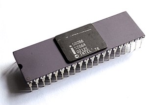
The 8086 is a 16-bit microprocessor chip designed by Intel between early 1976 and June 8, 1978, when it was released. The Intel 8088, released July 1, 1979, is a slightly modified chip with an external 8-bit data bus, and is notable as the processor used in the original IBM PC design.

<span class="mw-page-title-main">Zilog Z80</span> 8-bit microprocessor

The Z80 is an 8-bit microprocessor introduced by Zilog as the startup company's first product. The Z80 was conceived by Federico Faggin in late 1974 and developed by him and his 11 employees starting in early 1975. The first working samples were delivered in March 1976, and it was officially introduced on the market in July 1976. With the revenue from the Z80, the company built its own chip factories and grew to over a thousand employees over the following two years.

<span class="mw-page-title-main">Intel 8051</span> Single chip microcontroller series by Intel

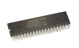
The Intel MCS-51 is a single chip microcontroller (MCU) series developed by Intel in 1980 for use in embedded systems. The architect of the Intel MCS-51 instruction set was John H. Wharton. Intel's original versions were popular in the 1980s and early 1990s, and enhanced binary compatible derivatives remain popular today. It is a complex instruction set computer, but also has some of the features of RISC architectures, such as a large register set and register windows, and has separate memory spaces for program instructions and data.

<span class="mw-page-title-main">Intel 8085</span> 8-bit microprocessor by Intel

The Intel 8085 ("eighty-eighty-five") is an 8-bit microprocessor produced by Intel and introduced in March 1976. It is software-binary compatible with the more-famous Intel 8080 with only two minor instructions added to support its added interrupt and serial input/output features. However, it requires less support circuitry, allowing simpler and less expensive microcomputer systems to be built. The "5" in the part number highlighted the fact that the 8085 uses a single +5-volt (V) power supply by using depletion-mode transistors, rather than requiring the +5 V, −5 V and +12 V supplies needed by the 8080. This capability matched that of the competing Z80, a popular 8080-derived CPU introduced the year before. These processors could be used in computers running the CP/M operating system.

x86 assembly language is the name for the family of assembly languages which provide some level of backward compatibility with CPUs back to the Intel 8008 microprocessor, which was launched in April 1972. It is used to produce object code for the x86 class of processors.

Addressing modes are an aspect of the instruction set architecture in most central processing unit (CPU) designs. The various addressing modes that are defined in a given instruction set architecture define how the machine language instructions in that architecture identify the operand(s) of each instruction. An addressing mode specifies how to calculate the effective memory address of an operand by using information held in registers and/or constants contained within a machine instruction or elsewhere.

The TMS9900 was one of the first commercially available, single-chip 16-bit microprocessors. Introduced in June 1976, it implemented Texas Instruments' TI-990 minicomputer architecture in a single-chip format, and was initially used for low-end models of that lineup.

<span class="mw-page-title-main">Fairchild F8</span> 8-bit microprocessor first shipped in 1975

The Fairchild F8 is an 8-bit microprocessor system from Fairchild Semiconductor, announced in 1974 and shipped in 1975. The original processor family included four main 40-pin integrated circuits (ICs); the 3850 CPU which was the arithmetic logic unit, the 3851 Program Storage Unit (PSU) which contained 1 KB of program ROM and handled instruction decoding, and the optional 3852 Dynamic Memory Interface (DMI) or 3853 Static Memory Interface (SMI) to control additional RAM or ROM holding the user programs or data. The 3854 DMA was another optional system that added direct memory access into the RAM controlled by the 3852.

<span class="mw-page-title-main">Signetics 2650</span> 8-bit microprocessor

The Signetics 2650 was an 8-bit microprocessor introduced in July 1975. According to Adam Osborne's book An Introduction to Microprocessors Vol 2: Some Real Products, it was "the most minicomputer-like" of the microprocessors available at the time. A combination of missing features and odd memory access limited its appeal, and the system saw little use in the market.

<span class="mw-page-title-main">WDC 65C02</span> CMOS microprocessor in the 6502 family

The Western Design Center (WDC) 65C02 microprocessor is an enhanced CMOS version of the popular nMOS-based 8-bit MOS Technology 6502. The 65C02 uses less power than the original 6502, fixes several problems, and adds new instructions. The power usage is on the order of 10 to 20 times less than the original 6502 running at the same speed; its reduced power consumption has made it useful in portable computer roles and industrial microcontroller systems. The 65C0s has also been used in some home computers, as well as in embedded applications, including medical-grade implanted devices.

<span class="mw-page-title-main">TI-990</span> Series of 16-bit computers by Texas Instruments.

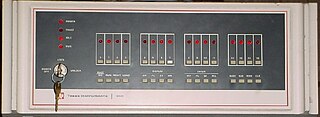
The TI-990 was a series of 16-bit minicomputers sold by Texas Instruments (TI) in the 1970s and 1980s. The TI-990 was a replacement for TI's earlier minicomputer systems, the TI-960 and the TI-980. It had several unique features, and was easier to program than its predecessors.

<span class="mw-page-title-main">General Instrument CP1600</span>

The CP1600 is a 16-bit microprocessor created in a partnership between General Instrument and Honeywell, introduced in February 1975. It is one of the first single-chip 16-bit processors. The overall design bore a strong resemblance to the PDP-11.

<span class="mw-page-title-main">National Semiconductor PACE</span>

National Semiconductor's IPC-16A PACE, short for "Processing and Control Element", was the first commercial single-chip 16-bit microprocessor, announced in late 1974. It was a single-chip implementation of their early 1973 five-chip IMP-16 architecture, which in turn had been inspired by the Data General Nova minicomputer. To the basic IMP-16, PACE added a new operational mode, "byte mode", which was useful for working with 8-bit data like ASCII text.

The PDP-11 architecture is a 16-bit CISC instruction set architecture (ISA) developed by Digital Equipment Corporation (DEC). It is implemented by central processing units (CPUs) and microprocessors used in PDP-11 minicomputers. It was in wide use during the 1970s, but was eventually overshadowed by the more powerful VAX architecture in the 1980s.

<span class="mw-page-title-main">WDC 65C816</span> 8/16-bit microprocessor

The W65C816S is a 16-bit microprocessor (MPU) developed and sold by the Western Design Center (WDC). Introduced in 1983, the W65C816S is an enhanced version of the WDC 65C02 8-bit MPU, itself a CMOS enhancement of the venerable MOS Technology 6502 NMOS MPU. The 65C816 is the CPU for the Apple IIGS and, in modified form, the Super Nintendo Entertainment System.

The Mostek MK5065 was an 8-bit microprocessor introduced by Mostek in early 1974. The design was originally developed by Motorola for use in an Olivetti electronic calculator, and was licensed to Mostek for use in non-calculator roles. It featured three sets of processor registers, allowing it to switch to an interrupt handler in a single cycle, and a wait-for-data mode that aided direct memory access.

<span class="mw-page-title-main">WD16</span> Processor produced by Western Digital

The WD16 is a 16-bit microprocessor introduced by Western Digital in October 1976. It is based on the MCP-1600 chipset, a general-purpose design that was also used to implement the DEC LSI-11 low-end minicomputer and the Pascal MicroEngine processor. The three systems differed primarily in their microcode, giving each system a unique instruction set architecture (ISA).

<span class="mw-page-title-main">COP400</span>

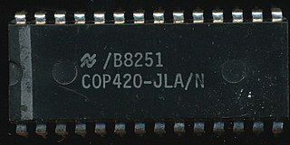
The COP400 or COP II is a 4-bit microcontroller family introduced in 1977 by National Semiconductor as a follow-on product to their original PMOS COP microcontroller. COP400 family members are complete microcomputers containing internal timing, logic, ROM, RAM, and I/O necessary to implement dedicated controllers. Some COP400 devices were second-sourced by Western Digital as the WD4200 family. In the Soviet Union several COP400 microcontrollers were manufactured as the 1820 series.

The MAC-8, better known today as the BELLMAC-8, is an 8-bit microprocessor designed by Bell Labs. Production began in CMOS form at Western Electric as the WE212 in 1977. The MAC-8 was used only in AT&T products, like the 4ESS. No commercial spec sheets were published, so it is little known as a result. The best-known use, in the public, is the MAC-TUTOR computer trainer, released in 1979.

References

Citations

Bibliography