In integrated circuit manufacturing, photolithography or optical lithography is a general term for techniques that use light to produce minutely patterned thin films of suitable materials over a substrate, such as a silicon wafer, to protect selected areas of it during subsequent etching, deposition, or implantation operations. Typically, ultraviolet light is used to transfer a geometric design from an optical mask to a light-sensitive chemical (photoresist) coated on the substrate. The photoresist either breaks down or hardens where it is exposed to light. The patterned film is then created by removing the softer parts of the coating with appropriate solvents.

An optical mouse is a computer mouse which uses a light source, typically a light-emitting diode (LED), and a light detector, such as an array of photodiodes, to detect movement relative to a surface. Variations of the optical mouse have largely replaced the older mechanical mouse design, which uses moving parts to sense motion.
A digital image is an image composed of picture elements, also known as pixels, each with finite, discrete quantities of numeric representation for its intensity or gray level that is an output from its two-dimensional functions fed as input by its spatial coordinates denoted with x, y on the x-axis and y-axis, respectively. Depending on whether the image resolution is fixed, it may be of vector or raster type. By itself, the term "digital image" usually refers to raster images or bitmapped images.

Optical coherence tomography (OCT) is an imaging technique that uses low-coherence light to capture micrometer-resolution, two- and three-dimensional images from within optical scattering media. It is used for medical imaging and industrial nondestructive testing (NDT). Optical coherence tomography is based on low-coherence interferometry, typically employing near-infrared light. The use of relatively long wavelength light allows it to penetrate into the scattering medium. Confocal microscopy, another optical technique, typically penetrates less deeply into the sample but with higher resolution.

A photomask is an opaque plate with holes or transparencies that allow light to shine through in a defined pattern. They are commonly used in photolithography and the production of integrated circuits in particular. Masks are used to produce a pattern on a substrate, normally a thin slice of silicon known as a wafer in the case of chip manufacturing. Several masks are used in turn, each one reproducing a layer of the completed design, and together they are known as a mask set.

Immersion lithography is a photolithography resolution enhancement technique for manufacturing integrated circuits (ICs) that replaces the usual air gap between the final lens and the wafer surface with a liquid medium that has a refractive index greater than one. The resolution is increased by a factor equal to the refractive index of the liquid. Current immersion lithography tools use highly purified water for this liquid, achieving feature sizes below 45 nanometers. ASML and Nikon are currently the only manufacturers of immersion lithography systems.
Chris Mack is an expert in photolithography. He received multiple undergraduate degrees from Rose-Hulman Institute of Technology in 1982, a master of science degree in electrical engineering from the University of Maryland, College Park in 1989, and a PhD in chemical engineering from The University of Texas in 1998.

Extreme ultraviolet lithography is an optical lithography technology using a range of extreme ultraviolet (EUV) wavelengths, roughly spanning a 2% FWHM bandwidth about 13.5 nm, to produce a pattern by exposing reflective photomask to UV light which gets reflected onto a substrate covered by photoresist. It is widely applied in semiconductor device fabrication process.
SPIE is an international not-for-profit professional society for optics and photonics technology, founded in 1955. It organizes technical conferences, trade exhibitions, and continuing education programs for researchers and developers in the light-based fields of physics, including: optics, photonics, and imaging engineering. The society publishes peer-reviewed scientific journals, conference proceedings, monographs, tutorial texts, field guides, and reference volumes in print and online. SPIE is especially well-known for Photonics West, one of the laser and photonics industry's largest combined conferences and tradeshows which is held annually in San Francisco. SPIE also participates as partners in leading educational initiatives, and in 2020, for example, provided more than $5.8 million in support of optics education and outreach programs around the world.

Phase-shift masks are photomasks that take advantage of the interference generated by phase differences to improve image resolution in photolithography. There exist alternating and attenuated phase shift masks. A phase-shift mask relies on the fact that light passing through a transparent media will undergo a phase change as a function of its optical thickness.
Optical proximity correction (OPC) is a photolithography enhancement technique commonly used to compensate for image errors due to diffraction or process effects. The need for OPC is seen mainly in the making of semiconductor devices and is due to the limitations of light to maintain the edge placement integrity of the original design, after processing, into the etched image on the silicon wafer. These projected images appear with irregularities such as line widths that are narrower or wider than designed, these are amenable to compensation by changing the pattern on the photomask used for imaging. Other distortions such as rounded corners are driven by the resolution of the optical imaging tool and are harder to compensate for. Such distortions, if not corrected for, may significantly alter the electrical properties of what was being fabricated. Optical proximity correction corrects these errors by moving edges or adding extra polygons to the pattern written on the photomask. This may be driven by pre-computed look-up tables based on width and spacing between features or by using compact models to dynamically simulate the final pattern and thereby drive the movement of edges, typically broken into sections, to find the best solution,. The objective is to reproduce on the semiconductor wafer, as well as possible, the original layout drawn by the designer.
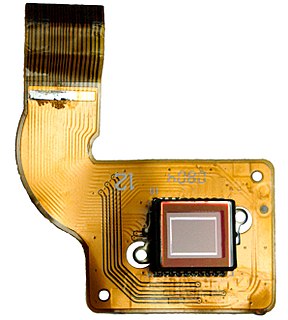
An image sensor or imager is a sensor that detects and conveys information used to make an image. It does so by converting the variable attenuation of light waves into signals, small bursts of current that convey the information. The waves can be light or other electromagnetic radiation. Image sensors are used in electronic imaging devices of both analog and digital types, which include digital cameras, camera modules, camera phones, optical mouse devices, medical imaging equipment, night vision equipment such as thermal imaging devices, radar, sonar, and others. As technology changes, electronic and digital imaging tends to replace chemical and analog imaging.
Contact lithography, also known as contact printing, is a form of photolithography whereby the image to be printed is obtained by illumination of a photomask in direct contact with a substrate coated with an imaging photoresist layer.
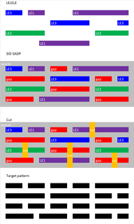
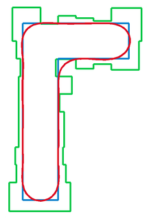
Multiple patterning is a class of technologies for manufacturing integrated circuits (ICs), developed for photolithography to enhance the feature density. It is expected to be necessary for the 10 nm and 7 nm node semiconductor processes and beyond. The premise is that a single lithographic exposure may not be enough to provide sufficient resolution. Hence additional exposures would be needed, or else positioning patterns using etched feature sidewalls would be necessary.
The 14 nm process refers to the MOSFET technology node that is the successor to the 22 nm node. The 14 nm was so named by the International Technology Roadmap for Semiconductors (ITRS). Until about 2011, the node following 22 nm was expected to be 16 nm. All 14 nm nodes use FinFET technology, a type of multi-gate MOSFET technology that is a non-planar evolution of planar silicon CMOS technology.
Computational lithography is the set of mathematical and algorithmic approaches designed to improve the resolution attainable through photolithography. Computational lithography has come to the forefront of photolithography in 2008 as the semiconductor industry grappled with the challenges associated with the transition to 22 nanometer CMOS process technology and beyond.
In semiconductor manufacturing, the International Technology Roadmap for Semiconductors defines the 7 nm process as the MOSFET technology node following the 10 nm node. It is based on FinFET technology, a type of multi-gate MOSFET technology.

Carl Zeiss SMT GmbH comprises the Semiconductor Manufacturing Technology business group of ZEISS and develops and produces equipment for the manufacture of microchips. The company is majority owned by Carl Zeiss AG, with a 24.9% minority stake by ASML Holding.
Peter Trefonas is a retired DuPont Fellow at DuPont, where he had worked on the development of electronic materials. He is known for innovations in the chemistry of photolithography, particularly the development of anti-reflective coatings and polymer photoresists that are used to create circuitry for computer chips. This work has supported the patterning of smaller features during the lithographic process, increasing miniaturization and microprocessor speed.
Orly Yadid-Pecht is a Professor of Electrical and Computer Engineering and Alberta Innovates Technology Futures Strategic Chair of Integrated Intelligent Sensors at the University of Calgary. She develops CMOS based imaging devices for biomedical sensing. She is a Fellow of the Institute of Electrical and Electronics Engineers, SPIE and American Institute for Medical and Biological Engineering. She is an ASTech Award Winner for Technology. Yadid-Pecht holds several patents for new technologies, including sensors, health monitoring devices and drug delivery systems.