
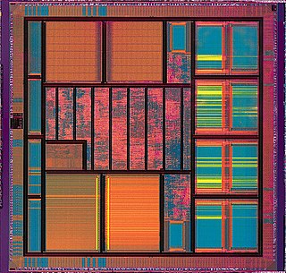
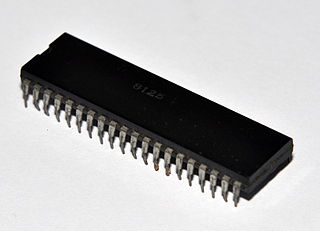
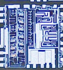
An integrated circuit or monolithic integrated circuit is a set of electronic circuits on one small flat piece of semiconductor material, usually silicon. Large numbers of tiny MOSFETs integrate into a small chip. This results in circuits that are orders of magnitude smaller, faster, and less expensive than those constructed of discrete electronic components. The IC's mass production capability, reliability, and building-block approach to integrated circuit design has ensured the rapid adoption of standardized ICs in place of designs using discrete transistors. ICs are now used in virtually all electronic equipment and have revolutionized the world of electronics. Computers, mobile phones, and other digital home appliances are now inextricable parts of the structure of modern societies, made possible by the small size and low cost of ICs such as modern computer processors and microcontrollers.
Very large-scale integration (VLSI) is the process of creating an integrated circuit (IC) by combining millions of MOS transistors onto a single chip. VLSI began in the 1970s when MOS integrated circuit chips were widely adopted, enabling complex semiconductor and telecommunication technologies to be developed. The microprocessor and memory chips are VLSI devices. Before the introduction of VLSI technology, most ICs had a limited set of functions they could perform. An electronic circuit might consist of a CPU, ROM, RAM and other glue logic. VLSI enables IC designers to add all of these into one chip.
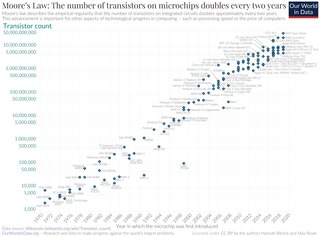
Moore's law is the observation that the number of transistors in a dense integrated circuit (IC) doubles about every two years. Moore's law is an observation and projection of a historical trend. Rather than a law of physics, it is an empirical relationship linked to gains from experience in production.

The metal–oxide–semiconductor field-effect transistor, also known as the metal–oxide–silicon transistor, is a type of insulated-gate field-effect transistor that is fabricated by the controlled oxidation of a semiconductor, typically silicon. The voltage of the covered gate determines the electrical conductivity of the device; this ability to change conductivity with the amount of applied voltage can be used for amplifying or switching electronic signals.
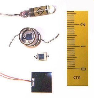
A photodiode is a semiconductor p–n junction device that converts light into an electrical current. The current is generated when photons are absorbed in the photodiode. Photodiodes may contain optical filters, built-in lenses, and may have large or small surface areas. Photodiodes usually have a slower response time as their surface area increases. The common, traditional solar cell used to generate electric solar power is a large area photodiode.
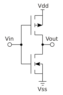
Complementary metal–oxide–semiconductor, also known as complementary-symmetry metal–oxide–semiconductor (COS-MOS), is a type of metal–oxide–semiconductor field-effect transistor (MOSFET) fabrication process that uses complementary and symmetrical pairs of p-type and n-type MOSFETs for logic functions. CMOS technology is used for constructing integrated circuit (IC) chips, including microprocessors, microcontrollers, memory chips, and other digital logic circuits. CMOS technology is also used for analog circuits such as image sensors, data converters, RF circuits, and highly integrated transceivers for many types of communication.
A nanowire is a nanostructure, with the diameter of the order of a nanometre (10−9 metres). More generally, nanowires can be defined as structures that have a thickness or diameter constrained to tens of nanometers or less and an unconstrained length. At these scales, quantum mechanical effects are important—which coined the term "quantum wires". Many different types of nanowires exist, including superconducting (e.g. YBCO), metallic (e.g. Ni, Pt, Au, Ag), semiconducting (e.g. silicon nanowires (SiNWs), InP, GaN) and insulating (e.g. SiO2, TiO2). Molecular nanowires are composed of repeating molecular units either organic (e.g. DNA) or inorganic (e.g. Mo6S9−xIx).
A gate array is an approach to the design and manufacture of application-specific integrated circuits (ASICs) using a prefabricated chip with components that are later interconnected into logic devices according to a custom order by adding metal interconnect layers in the factory. It was popular during upheaval in semiconductor industry in 80s and its usage declined by end of 90s.

Nanoelectromechanical systems (NEMS) are a class of devices integrating electrical and mechanical functionality on the nanoscale. NEMS form the next logical miniaturization step from so-called microelectromechanical systems, or MEMS devices. NEMS typically integrate transistor-like nanoelectronics with mechanical actuators, pumps, or motors, and may thereby form physical, biological, and chemical sensors. The name derives from typical device dimensions in the nanometer range, leading to low mass, high mechanical resonance frequencies, potentially large quantum mechanical effects such as zero point motion, and a high surface-to-volume ratio useful for surface-based sensing mechanisms. Applications include accelerometers and sensors to detect chemical substances in the air.
In computer engineering, a logic family is one of two related concepts:
A mixed-signal integrated circuit is any integrated circuit that has both analog circuits and digital circuits on a single semiconductor die.
Nanochemistry is the combination of chemistry and nano science. Nanochemistry is associated with synthesis of building blocks which are dependent on size, surface, shape and defect properties. Nanochemistry is being used in chemical, materials and physical, science as well as engineering, biological and medical applications. Nanochemistry and other nanoscience fields have the same core concepts but the usages of those concepts are different.
A field-programmable analog array (FPAA) is an integrated circuit device containing computational analog blocks (CAB) and interconnects between these blocks offering field-programmability. Unlike their digital cousin, the FPGA, the devices tend to be more application driven than general purpose as they may be current mode or voltage mode devices. For voltage mode devices, each block usually contains an operational amplifier in combination with programmable configuration of passive components. The blocks can, for example, act as summers or integrators.
Nanoelectronics refers to the use of nanotechnology in electronic components. The term covers a diverse set of devices and materials, with the common characteristic that they are so small that inter-atomic interactions and quantum mechanical properties need to be studied extensively. Some of these candidates include: hybrid molecular/semiconductor electronics, one-dimensional nanotubes/nanowires or advanced molecular electronics.

A multigate device, multi-gate MOSFET or multi-gate field-effect transistor (MuGFET) refers to a metal–oxide–semiconductor field-effect transistor (MOSFET) that has more than one gate into a single device. The multiple gates may be controlled by a single gate electrode, wherein the multiple gate surfaces act electrically as a single gate, or by independent gate electrodes. A multigate device employing independent gate electrodes is sometimes called a multiple-independent-gate field-effect transistor (MIGFET). The most widely used multi-gate devices are the FinFET and the GAAFET, which are non-planar transistors, or 3D transistors.
Nanocircuits are electrical circuits operating on the nanometer scale. This is well into the quantum realm, where quantum mechanical effects become very important. One nanometer is equal to 10−9 meters or a row of 10 hydrogen atoms. With such progressively smaller circuits, more can be fitted on a computer chip. This allows faster and more complex functions using less power. Nanocircuits are composed of three different fundamental components. These are transistors, interconnections, and architecture, all fabricated on the nanometer scale.
Computing with Memory refers to computing platforms where function response is stored in memory array, either one or two-dimensional, in the form of lookup tables (LUTs) and functions are evaluated by retrieving the values from the LUTs. These computing platforms can follow either a purely spatial computing model, as in field-programmable gate array (FPGA), or a temporal computing model, where a function is evaluated across multiple clock cycles. The latter approach aims at reducing the overhead of programmable interconnect in FPGA by folding interconnect resources inside a computing element. It uses dense two-dimensional memory arrays to store large multiple-input multiple-output LUTs. Computing with Memory differs from Computing in Memory or processor-in-memory (PIM) concepts, widely investigated in the context of integrating a processor and memory on the same chip to reduce memory latency and increase bandwidth. These architectures seek to reduce the distance the data travels between the processor and the memory. The Berkeley IRAM project is one notable contribution in the area of PIM architectures.
The IEEE International Electron Devices Meeting (IEDM) is an annual micro- and nanoelectronics conference held each December that serves as a forum for reporting technological breakthroughs in the areas of semiconductor and related device technologies, design, manufacturing, physics, modeling and circuit-device interaction.

The field-effect transistor (FET) is a type of transistor that uses an electric field to control the flow of current in a semiconductor. FETs are devices with three terminals: source, gate, and drain. FETs control the flow of current by the application of a voltage to the gate, which in turn alters the conductivity between the drain and source.
RF CMOS is a metal–oxide–semiconductor (MOS) integrated circuit (IC) technology that integrates radio-frequency (RF), analog and digital electronics on a mixed-signal CMOS RF circuit chip. It is widely used in modern wireless telecommunications, such as cellular networks, Bluetooth, Wi-Fi, GPS receivers, broadcasting, vehicular communication systems, and the radio transceivers in all modern mobile phones and wireless networking devices. RF CMOS technology was pioneered by Pakistani engineer Asad Ali Abidi at UCLA during the late 1980s to early 1990s, and helped bring about the wireless revolution with the introduction of digital signal processing in wireless communications. The development and design of RF CMOS devices was enabled by van der Ziel's FET RF noise model, which was published in the early 1960s and remained largely forgotten until the 1990s.