Related Research Articles

The atomic number or proton number of a chemical element is the number of protons found in the nucleus of every atom of that element. The atomic number uniquely identifies a chemical element. It is identical to the charge number of the nucleus. In an uncharged atom, the atomic number is also equal to the number of electrons.

The cathode-ray tube (CRT) is a vacuum tube that contains one or more electron guns and a phosphorescent screen and is used to display images. It modulates, accelerates, and deflects electron beam(s) onto the screen to create the images. The images may represent electrical waveforms (oscilloscope), pictures, radar targets, or other phenomena. CRTs have also been used as memory devices, in which case the visible light emitted from the fluorescent material is not intended to have significant meaning to a visual observer.

An electric current is the rate of flow of electric charge past a point or region. An electric current is said to exist when there is a net flow of electric charge through a region. In electric circuits this charge is often carried by electrons moving through a wire. It can also be carried by ions in an electrolyte, or by both ions and electrons such as in an ionized gas (plasma).

A scanning electron microscope (SEM) is a type of electron microscope that produces images of a sample by scanning the surface with a focused beam of electrons. The electrons interact with atoms in the sample, producing various signals that contain information about the surface topography and composition of the sample. The electron beam is scanned in a raster scan pattern, and the position of the beam is combined with the intensity of the detected signal to produce an image. In the most common SEM mode, secondary electrons emitted by atoms excited by the electron beam are detected using a secondary electron detector. The number of secondary electrons that can be detected, and thus the signal intensity, depends, among other things, on specimen topography. SEM can achieve resolution better than 1 nanometer.
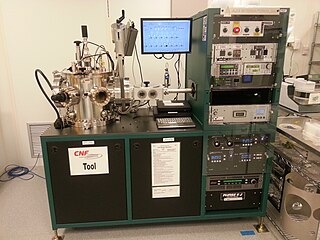
In physics, sputtering is a phenomenon in which microscopic particles of a solid material are ejected from its surface, after the material is itself bombarded by energetic particles of a plasma or gas. It occurs naturally in outer space, and can be an unwelcome source of wear in precision components. However, the fact that it can be made to act on extremely fine layers of material is exploited in science and industry—there, it is used to perform precise etching, carry out analytical techniques, and deposit thin film layers in the manufacture of optical coatings, semiconductor devices and nanotechnology products.

Static electricity is an imbalance of electric charges within or on the surface of a material. The charge remains until it is able to move away by means of an electric current or electrical discharge. Static electricity is named in contrast with current electricity, which flows through wires or other conductors and transmits energy.

The Selectron was an early form of digital computer memory developed by Jan A. Rajchman and his group at the Radio Corporation of America (RCA) under the direction of Vladimir K. Zworykin. It was a vacuum tube that stored digital data as electrostatic charges using technology similar to the Williams tube storage device. The team was never able to produce a commercially viable form of Selectron before magnetic-core memory became almost universal, and it remains practically unknown today.

A corona discharge is an electrical discharge brought on by the ionization of a fluid such as air surrounding a conductor that is electrically charged. Spontaneous corona discharges occur naturally in high-voltage systems unless care is taken to limit the electric field strength. A corona will occur when the strength of the electric field around a conductor is high enough to form a conductive region, but not high enough to cause electrical breakdown or arcing to nearby objects. It is often seen as a bluish glow in the air adjacent to pointed metal conductors carrying high voltages, and emits light by the same property as a gas discharge lamp.

Video camera tubes were devices based on the cathode ray tube that were used to capture television images prior to the introduction of charge-coupled device (CCD) image sensors in the 1980s. Several different types of tubes were in use from the early 1930s to the 1980s.
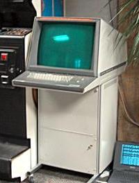
Storage tubes are a class of cathode-ray tubes (CRTs) that are designed to hold an image for a long period of time, typically as long as power is supplied to the tube.
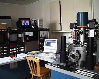
Electron-beam lithography is the practice of scanning a focused beam of electrons to draw custom shapes on a surface covered with an electron-sensitive film called a resist (exposing). The electron beam changes the solubility of the resist, enabling selective removal of either the exposed or non-exposed regions of the resist by immersing it in a solvent (developing). The purpose, as with photolithography, is to create very small structures in the resist that can subsequently be transferred to the substrate material, often by etching.

Direct-view bistable storage tube (DVBST) was an acronym used by Tektronix to describe their line of storage tubes. These were cathode ray tubes (CRT) that stored information written to them using an analog technique inherent in the CRT and based upon the secondary emission of electrons from the phosphor screen itself. The resulting image was visible in the continuously glowing patterns on the face of the CRT.
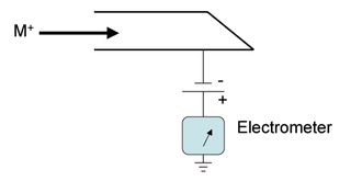
A Faraday cup is a metal (conductive) cup designed to catch charged particles in vacuum. The resulting current can be measured and used to determine the number of ions or electrons hitting the cup. The Faraday cup was named after Michael Faraday who first theorized ions around 1830.
A particle-beam weapon uses a high-energy beam of atomic or subatomic particles to damage the target by disrupting its atomic and/or molecular structure. A particle-beam weapon is a type of directed-energy weapon, which directs energy in a particular and focused direction using particles with minuscule mass. Some particle-beam weapons have potential practical applications, e.g. as an antiballistic missile defense system for the United States and its cancelled Strategic Defense Initiative. They have been known by myriad names: phasers, particle accelerator guns, ion cannons, proton beams, lightning rays, rayguns, etc.

Extreme ultraviolet radiation or high-energy ultraviolet radiation is electromagnetic radiation in the part of the electromagnetic spectrum spanning wavelengths from 124 nm down to 10 nm, and therefore having photons with energies from 10 eV up to 124 eV. EUV is naturally generated by the solar corona and artificially by plasma and synchrotron light sources. Since UVC extends to 100 nm, there is some overlap in the terms.
Migma, sometimes migmatron or migmacell, was a proposed colliding beam fusion reactor designed by Bogdan Maglich in 1969. Migma uses self-intersecting beams of ions from small particle accelerators to force the ions to fuse. Similar systems using larger collections of particles, up to microscopic dust sized, were referred to as "macrons". Migma was an area of some research in the 1970s and early 1980s, but lack of funding precluded further development.

Sputter deposition is a physical vapor deposition (PVD) method of thin film deposition by sputtering. This involves ejecting material from a "target" that is a source onto a "substrate" such as a silicon wafer. Resputtering is re-emission of the deposited material during the deposition process by ion or atom bombardment. Sputtered atoms ejected from the target have a wide energy distribution, typically up to tens of eV. The sputtered ions can ballistically fly from the target in straight lines and impact energetically on the substrates or vacuum chamber. Alternatively, at higher gas pressures, the ions collide with the gas atoms that act as a moderator and move diffusively, reaching the substrates or vacuum chamber wall and condensing after undergoing a random walk. The entire range from high-energy ballistic impact to low-energy thermalized motion is accessible by changing the background gas pressure. The sputtering gas is often an inert gas such as argon. For efficient momentum transfer, the atomic weight of the sputtering gas should be close to the atomic weight of the target, so for sputtering light elements neon is preferable, while for heavy elements krypton or xenon are used. Reactive gases can also be used to sputter compounds. The compound can be formed on the target surface, in-flight or on the substrate depending on the process parameters. The availability of many parameters that control sputter deposition make it a complex process, but also allow experts a large degree of control over the growth and microstructure of the film.

Low-energy ion scattering spectroscopy (LEIS), sometimes referred to simply as ion scattering spectroscopy (ISS), is a surface-sensitive analytical technique used to characterize the chemical and structural makeup of materials. LEIS involves directing a stream of charged particles known as ions at a surface and making observations of the positions, velocities, and energies of the ions that have interacted with the surface. Data that is thus collected can be used to deduce information about the material such as the relative positions of atoms in a surface lattice and the elemental identity of those atoms. LEIS is closely related to both medium-energy ion scattering (MEIS) and high-energy ion scattering, differing primarily in the energy range of the ion beam used to probe the surface. While much of the information collected using LEIS can be obtained using other surface science techniques, LEIS is unique in its sensitivity to both structure and composition of surfaces. Additionally, LEIS is one of a very few surface-sensitive techniques capable of directly observing hydrogen atoms, an aspect that may make it an increasingly more important technique as the hydrogen economy is being explored.

X-ray lithography, is a process used in electronic industry to selectively remove parts of a thin film. It uses X-rays to transfer a geometric pattern from a mask to a light-sensitive chemical photoresist, or simply "resist," on the substrate. A series of chemical treatments then engraves the produced pattern into the material underneath the photoresist.
This is a subdivision of the Oscilloscope article, discussing the various types and models of oscilloscopes in greater detail.
References
- Barnard, B. R. "Flood Gun for Charge Neutralization", 2005