
Semiconductor device fabrication is the process used to manufacture semiconductor devices, typically integrated circuits (ICs) such as computer processors, microcontrollers, and memory chips that are present in everyday electrical and electronic devices. It is a multiple-step photolithographic and physio-chemical process during which electronic circuits are gradually created on a wafer, typically made of pure single-crystal semiconducting material. Silicon is almost always used, but various compound semiconductors are used for specialized applications.

In electronics, a wafer is a thin slice of semiconductor, such as a crystalline silicon (c-Si), used for the fabrication of integrated circuits and, in photovoltaics, to manufacture solar cells. The wafer serves as the substrate for microelectronic devices built in and upon the wafer. It undergoes many microfabrication processes, such as doping, ion implantation, etching, thin-film deposition of various materials, and photolithographic patterning. Finally, the individual microcircuits are separated by wafer dicing and packaged as an integrated circuit.

A fishing line is a flexible, high-tensile cord used in angling to tether and pull in fish, in conjunction with at least one hook. Fishing lines are usually pulled by and stored in a reel, but can also be retrieved by hand, with a fixed attachment to the end of a rod, or via a motor.

STMicroelectronics N.V. commonly referred to as ST or STMicro is a multinational corporation and technology company of French-Italian origin headquartered in Plan-les-Ouates near Geneva, Switzerland and listed on the New York Stock Exchange, on the Euronext Paris in Paris and on the Borsa Italiana in Milan. ST is the largest European semiconductor contract manufacturing and design company. The company resulted from the merger of two government-owned semiconductor companies in 1987: Thomson Semiconducteurs of France and SGS Microelettronica of Italy.

The Czochralski method, also Czochralski technique or Czochralski process, is a method of crystal growth used to obtain single crystals of semiconductors, metals, salts and synthetic gemstones. The method is named after Polish scientist Jan Czochralski, who invented the method in 1915 while investigating the crystallization rates of metals. He made this discovery by accident: instead of dipping his pen into his inkwell, he dipped it in molten tin, and drew a tin filament, which later proved to be a single crystal. The method is still used in over 90 percent of all electronics in the world that use semiconductors.

Polyvinylidene fluoride or polyvinylidene difluoride (PVDF) is a highly non-reactive thermoplastic fluoropolymer produced by the polymerization of vinylidene difluoride. Its chemical formula is (C2H2F2)n.

Purified water is water that has been mechanically filtered or processed to remove impurities and make it suitable for use. Distilled water was, formerly, the most common form of purified water, but, in recent years, water is more frequently purified by other processes including capacitive deionization, reverse osmosis, carbon filtering, microfiltration, ultrafiltration, ultraviolet oxidation, or electrodeionization. Combinations of a number of these processes have come into use to produce ultrapure water of such high purity that its trace contaminants are measured in parts per billion (ppb) or parts per trillion (ppt).

A stepper is a device used in the manufacture of integrated circuits (ICs) that is similar in operation to a slide projector or a photographic enlarger. Stepper is short for step-and-repeat camera. Steppers are an essential part of the complex process, called photolithography, which creates millions of microscopic circuit elements on the surface of silicon wafers out of which chips are made. These chips form the heart of ICs such as computer processors, memory chips, and many other devices.

Float-zone silicon is very pure silicon obtained by vertical zone melting. The process was developed at Bell Labs by Henry Theuerer in 1955 as a modification of a method developed by William Gardner Pfann for germanium. In the vertical configuration molten silicon has sufficient surface tension to keep the charge from separating. The major advantages is crucibleless growth that prevents contamination of the silicon from the vessel itself and therefore an inherently high-purity alternative to boule crystals grown by the Czochralski method.
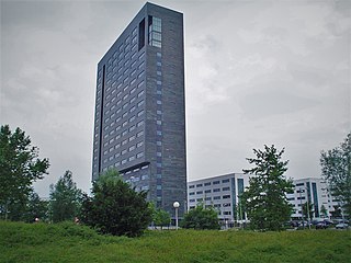
ASML Holding N.V. is a Dutch multinational corporation founded in 1984. ASML specializes in the development and manufacturing of photolithography machines which are used to produce computer chips.
The etch pit density (EPD) is a measure for the quality of semiconductor wafers.
Soitec is an international company based in France, that manufactures substrates used in the creation of semiconductors.
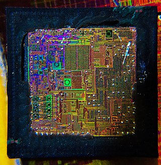
A die, in the context of integrated circuits, is a small block of semiconducting material on which a given functional circuit is fabricated. Typically, integrated circuits are produced in large batches on a single wafer of electronic-grade silicon (EGS) or other semiconductor through processes such as photolithography. The wafer is cut (diced) into many pieces, each containing one copy of the circuit. Each of these pieces is called a die.

Plastic pipe is a tubular section, or hollow cylinder, made of plastic. It is usually, but not necessarily, of circular cross-section, used mainly to convey substances which can flow—liquids and gases (fluids), slurries, powders and masses of small solids. It can also be used for structural applications; hollow pipes are far stiffer per unit weight than solid members.
A double-walled pipe is a secondary contained piping system. It is a pipe within a pipe, or encased in an outer covering, with an annulus between the two diameters. The inner pipe is the primary or carrier pipe and the outer pipe is called the secondary or containment pipe. The great majority of double-walled piping applications involve wastewater, groundwater, and process safety.
Wafer backgrinding is a semiconductor device fabrication step during which wafer thickness is reduced to allow stacking and high-density packaging of integrated circuits (IC).

A tube, or tubing, is a long hollow cylinder used for moving fluids or to protect electrical or optical cables and wires.
Ultra-high-purity steam, also called the clean steam, UHP steam or high purity water vapor, is used in a variety of industrial manufacturing processes that require oxidation or annealing. These processes include the growth of oxide layers on silicon wafers for the semiconductor industry, originally described by the Deal-Grove model, and for the formation of passivation layers used to improve the light capture ability of crystalline photovoltaic cells. Several methods and technologies can be employed to generate ultra high purity steam, including pyrolysis, bubbling, direct liquid injection, and purified steam generation. The level of purity, or the relative lack of contamination, affects the quality of the oxide layer or annealed surface. The method of delivery affects growth rate, uniformity, and electrical performance. Oxidation and annealing are common steps in the manufacture of such devices as microelectronics and solar cells.
Ultrapure water (UPW), high-purity water or highly purified water (HPW) is water that has been purified to uncommonly stringent specifications. Ultrapure water is a term commonly used in manufacturing to emphasize the fact that the water is treated to the highest levels of purity for all contaminant types, including: organic and inorganic compounds; dissolved and particulate matter; volatile and non-volatile; reactive, and inert; hydrophilic and hydrophobic; and dissolved gases.

Tower Semiconductor Ltd. is an Israeli company that manufactures integrated circuits using specialty process technologies, including SiGe, BiCMOS, Silicon Photonics, SOI, mixed-signal and RFCMOS, CMOS image sensors, non-imaging sensors, power management (BCD), and non-volatile memory (NVM) as well as MEMS capabilities. Tower Semiconductor also owns 51% of TPSCo, an enterprise with Nuvoton Technology Corporation Japan (NTCJ).

