External links
| General | |
|---|---|
| National libraries | |
| Other | |
Leigh Canham is a British scientist who has pioneered the optoelectronic and biomedical applications of porous silicon.
Leigh Canham graduated from University College London in 1979 with a BSc in Physics and completed his PhD at King's College London in 1983.
His early work in this area took place at the Royal Signals and Radar Establishment in Malvern, Worcestershire. Canham and his colleagues showed that electrochemically etched silicon could be made porous. This porous material could emit visible light when a current was passed through it (electroluminescence). Later the group demonstrated the biocompatibility of porous silicon.
Canham now works as Chief Scientific Officer of psiMedica (part of pSiVida). According to the pSiVida web site, Canham is the most cited author on porous silicon. In a study of most cited physicists up to 1997 Canham ranked at 771.
| General | |
|---|---|
| National libraries | |
| Other | |
A thin-film transistor (TFT) is a special type of field-effect transistor (FET) where the transistor is thin relative to the plane of the device. TFTs are grown on a supporting substrate. A common substrate is glass, because the traditional application of TFTs is in liquid-crystal displays (LCDs). This differs from the conventional bulk metal oxide field effect transistor (MOSFET), where the semiconductor material typically is the substrate, such as a silicon wafer.
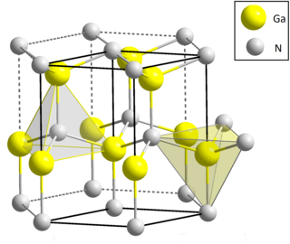
Gallium nitride is a binary III/V direct bandgap semiconductor commonly used in blue light-emitting diodes since the 1990s. The compound is a very hard material that has a Wurtzite crystal structure. Its wide band gap of 3.4 eV affords it special properties for applications in optoelectronic, high-power and high-frequency devices. For example, GaN is the substrate which makes violet (405 nm) laser diodes possible, without requiring nonlinear optical frequency-doubling.
In semiconductor manufacturing, silicon on insulator (SOI) technology is fabrication of silicon semiconductor devices in a layered silicon–insulator–silicon substrate, to reduce parasitic capacitance within the device, thereby improving performance. SOI-based devices differ from conventional silicon-built devices in that the silicon junction is above an electrical insulator, typically silicon dioxide or sapphire. The choice of insulator depends largely on intended application, with sapphire being used for high-performance radio frequency (RF) and radiation-sensitive applications, and silicon dioxide for diminished short-channel effects in other microelectronics devices. The insulating layer and topmost silicon layer also vary widely with application.
In materials science, the sol–gel process is a method for producing solid materials from small molecules. The method is used for the fabrication of metal oxides, especially the oxides of silicon (Si) and titanium (Ti). The process involves conversion of monomers into a colloidal solution (sol) that acts as the precursor for an integrated network of either discrete particles or network polymers. Typical precursors are metal alkoxides.
Porous silicon is a form of the chemical element silicon that has introduced nanopores in its microstructure, rendering a large surface to volume ratio in the order of 500 m2/cm3.
Atomic layer deposition (ALD) is a thin-film deposition technique based on the sequential use of a gas-phase chemical process; it is a subclass of chemical vapour deposition. The majority of ALD reactions use two chemicals called precursors. These precursors react with the surface of a material one at a time in a sequential, self-limiting, manner. A thin film is slowly deposited through repeated exposure to separate precursors. ALD is a key process in fabricating semiconductor devices, and part of the set of tools for synthesising nanomaterials.
Nanoarchitectures for lithium-ion batteries are attempts to employ nanotechnology to improve the design of lithium-ion batteries. Research in lithium-ion batteries focuses on improving energy density, power density, safety, durability and cost.
Carbide-derived carbon (CDC), also known as tunable nanoporous carbon, is the common term for carbon materials derived from carbide precursors, such as binary (e.g. SiC, TiC), or ternary carbides, also known as MAX phases (e.g., Ti2AlC, Ti3SiC2). CDCs have also been derived from polymer-derived ceramics such as Si-O-C or Ti-C, and carbonitrides, such as Si-N-C. CDCs can occur in various structures, ranging from amorphous to crystalline carbon, from sp2- to sp3-bonded, and from highly porous to fully dense. Among others, the following carbon structures have been derived from carbide precursors: micro- and mesoporous carbon, amorphous carbon, carbon nanotubes, onion-like carbon, nanocrystalline diamond, graphene, and graphite. Among carbon materials, microporous CDCs exhibit some of the highest reported specific surface areas (up to more than 3000 m2/g). By varying the type of the precursor and the CDC synthesis conditions, microporous and mesoporous structures with controllable average pore size and pore size distributions can be produced. Depending on the precursor and the synthesis conditions, the average pore size control can be applied at sub-Angstrom accuracy. This ability to precisely tune the size and shapes of pores makes CDCs attractive for selective sorption and storage of liquids and gases (e.g., hydrogen, methane, CO2) and the high electric conductivity and electrochemical stability allows these structures to be effectively implemented in electrical energy storage and capacitive water desalinization.

Crystalline silicon (c-Si) is the crystalline forms of silicon, either polycrystalline silicon, or monocrystalline silicon. Crystalline silicon is the dominant semiconducting material used in photovoltaic technology for the production of solar cells. These cells are assembled into solar panels as part of a photovoltaic system to generate solar power from sunlight.
Nanoneedles may be conical or tubular needles in the nanometre size range, made from silicon or boron-nitride with a central bore of sufficient size to allow the passage of large molecules, or solid needles useful in Raman spectroscopy, light emitting diodes (LED) and laser diodes.
James R. "Bob" Biard is an American electrical engineer and inventor who holds 73 U.S. patents. Some of his more significant patents include the first infrared light-emitting diode (LED), the optical isolator, Schottky clamped logic circuits, silicon Metal Oxide Semiconductor Read Only Memory, a low bulk leakage current avalanche photodetector, and fiber-optic data links. He has been on the staff of Texas A&M University as an Adjunct Professor of Electrical Engineering since 1980.
Research in lithium-ion batteries has produced many proposed refinements of lithium-ion batteries. Areas of research interest have focused on improving energy density, safety, rate capability, cycle durability, flexibility, and cost.
Michael J. Sailor is a nanotechnology researcher and professor at the University of California, San Diego. Sailor is best known for his research on porous silicon, a nanostructured material that is prepared by electrochemical corrosion of crystalline silicon wafers.
Low-temperature polycrystalline silicon (LTPS) is polycrystalline silicon that has been synthesized at relatively low temperatures compared to in traditional methods. LTPS is important for display industries, since the use of large glass panels prohibits exposure to deformative high temperatures. More specifically, the use of polycrystalline silicon in thin-film transistors (LTPS-TFT) has high potential for large-scale production of electronic devices like flat panel LCD displays or image sensors.
Mauro Ferrari is a nanoscientist and leader in the field of nanomedicine. He served as special expert on nanotechnology for the National Cancer Institute (2003-2005) and was instrumental in establishing the Alliance for Nanotechnology in Cancer in 2004. On 1 January 2020, Ferrari was made president of the European Research Council (ERC). Following a vote of no confidence, on 27 March 2020, "all 19 active members of the ERC’s Scientific Council individually and unanimously requested that Mauro Ferrari resign from his position as ERC’s President", due to poor conduct in office, exploiting the position to further his own projects, and for consistently failing to represent the interests of the ERC. On 7 April 2020, Ferrari officially resigned, stating to the media that he was "extremely disappointed by the European response” to the pandemic and expressing frustration over opposition to his efforts to launch a scientific program to combat the virus.
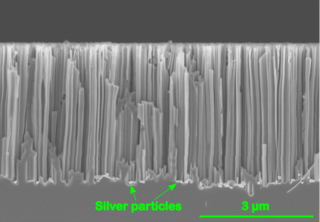
Metal Assisted Chemical Etching is the process of wet chemical etching of semiconductors with the use of a metal catalyst, usually deposited on the surface of a semiconductor in the form of a thin film or nanoparticles. The semiconductor, covered with the metal is then immersed in an etching solution containing and oxidizing agent and hydrofluoric acid. The metal on the surface catalyzes the reduction of the oxidizing agent and therefore in turn also the dissolution of silicon. In the majority of the conducted research this phenomenon of increased dissolution rate is also spatially confined, such that it is increased in close proximity to a metal particle at the surface. Eventually this leads to the formation of straight pores that are etched into the semiconductor. This means that a pre-defined pattern of the metal on the surface can be directly transferred to a semiconductor substrate.

Hexamethylcyclotrisilazane is a chemical compound with formula C
6H
21N
3Si
3 or [–Si(CH
3)
2–NH–]
3. Its molecule consists of a six-member ring of three silicon atoms alternating with three nitrogen atoms, with two methyl groups bonded to each silicon and one hydrogen atom bonded to each nitrogen. It can be described as a derivative of the hypothetical compound cyclotrisilazane [–SiH
2–NH–]
3, or as a cyclic trimer of hypothetical dimethylsilazane (CH
3)
2SiNH.
Francesca Iacopi is an engineer, researcher and an academic. She specializes in materials and nanoelectronics engineering and is a Professor at the University of Technology Sydney. She is a chief investigator of the ARC Centre of Excellence in Transformative Meta-Optical Systems, a Fellow of the Institution of Engineers Australia, and a senior member of Institute of Electrical and Electronics Engineers.
Silicon quantum dots are metal-free biologically compatible quantum dots with photoluminescence emission maxima that are tunable through the visible to near-infrared spectral regions. These quantum dots have unique properties arising from their indirect band gap, including long-lived luminescent excited-states and large Stokes shifts. A variety of disproportionation, pyrolysis, and solution protocols have been used to prepare silicon quantum dots, however it is important to note that some solution-based protocols for preparing luminescent silicon quantum dots actually yield carbon quantum dots instead of the reported silicon. The unique properties of silicon quantum dots lend themselves to an array of potential applications: biological imaging, luminescent solar concentrators, light emitting diodes, sensors, and lithium-ion battery anodes.