An amplifier, electronic amplifier or (informally) amp is an electronic device that can increase the magnitude of a signal. It is a two-port electronic circuit that uses electric power from a power supply to increase the amplitude of a signal applied to its input terminals, producing a proportionally greater amplitude signal at its output. The amount of amplification provided by an amplifier is measured by its gain: the ratio of output voltage, current, or power to input. An amplifier is defined as a circuit that has a power gain greater than one.

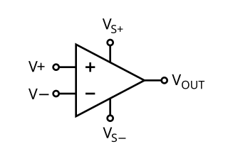
An operational amplifier is a DC-coupled electronic voltage amplifier with a differential input, a (usually) single-ended output, and an extremely high gain. Its name comes from its original use of performing mathematical operations in analog computers.

An instrumentation amplifier is a type of differential amplifier that has been outfitted with input buffer amplifiers, which eliminate the need for input impedance matching and thus make the amplifier particularly suitable for use in measurement and test equipment. Additional characteristics include very low DC offset, low drift, low noise, very high open-loop gain, very high common-mode rejection ratio, and very high input impedances. Instrumentation amplifiers are used where great accuracy and stability of the circuit both short- and long-term are required.

A differential amplifier is a type of electronic amplifier that amplifies the difference between two input voltages but suppresses any voltage common to the two inputs. It is an analog circuit with two inputs and and one output , in which the output is ideally proportional to the difference between the two voltages:

In electronics, a common-emitter amplifier is one of three basic single-stage bipolar-junction-transistor (BJT) amplifier topologies, typically used as a voltage amplifier. It offers high current gain, medium input resistance and a high output resistance. The output of a common emitter amplifier is inverted; i.e. for a sine wave input signal, the output signal is 180 degrees out of phase with respect to the input.

A current source is an electronic circuit that delivers or absorbs an electric current which is independent of the voltage across it.

A push–pull amplifier is a type of electronic circuit that uses a pair of active devices that alternately supply current to, or absorb current from, a connected load. This kind of amplifier can enhance both the load capacity and switching speed.
An integrator in measurement and control applications is an element whose output signal is the time integral of its input signal. It accumulates the input quantity over a defined time to produce a representative output.

A low-dropout regulator is a type of a DC linear voltage regulator circuit that can operate even when the supply voltage is very close to the output voltage. The advantages of an LDO regulator over other DC-to-DC voltage regulators include: the absence of switching noise ; smaller device size ; and greater design simplicity. The disadvantage is that linear DC regulators must dissipate heat in order to operate.
This article illustrates some typical operational amplifier applications. A non-ideal operational amplifier's equivalent circuit has a finite input impedance, a non-zero output impedance, and a finite gain. A real op-amp has a number of non-ideal features as shown in the diagram, but here a simplified schematic notation is used, many details such as device selection and power supply connections are not shown. Operational amplifiers are optimised for use with negative feedback, and this article discusses only negative-feedback applications. When positive feedback is required, a comparator is usually more appropriate. See Comparator applications for further information.

Clipping is a form of waveform distortion that occurs when an amplifier is overdriven and attempts to deliver an output voltage or current beyond its maximum capability. Driving an amplifier into clipping may cause it to output power in excess of its power rating.

In electronics, the Sziklai pair, also known as a complementary feedback pair, is a configuration of two bipolar transistors, similar to a Darlington pair. In contrast to the Darlington arrangement, the Sziklai pair has one NPN and one PNP transistor, and so it is sometimes also called the "complementary Darlington". The configuration is named for George C. Sziklai, thought to be its inventor.
Gain compression is a reduction in differential or slope gain caused by nonlinearity of the transfer function of an amplifying device for large-signal inputs.
A Wilson current mirror is a three-terminal circuit that accepts an input current at the input terminal and provides a "mirrored" current source or sink output at the output terminal. The mirrored current is a precise copy of the input current. It may be used as a Wilson current source by applying a constant bias current to the input branch as in Fig. 2. The circuit is named after George R. Wilson, an integrated circuit design engineer who worked for Tektronix. Wilson devised this configuration in 1967 when he and Barrie Gilbert challenged each other to find an improved current mirror overnight that would use only three transistors. Wilson won the challenge.

A multistage amplifier is an electronic amplifier consisting of two or more single-stage amplifiers connected together. In this context, a single stage is an amplifier containing only a single transistor or other active device. The most common reason for using multiple stages is to increase the gain of the amplifier in applications where the input signal is very small, for instance in radio receivers. In these applications a single stage has insufficient gain by itself. In some designs it is possible to obtain more desirable values of other parameters such as input resistance and output resistance.
A fully differential amplifier (FDA) is a DC-coupled high-gain electronic voltage amplifier with differential inputs and differential outputs. In its ordinary usage, the output of the FDA is controlled by two feedback paths which, because of the amplifier's high gain, almost completely determine the output voltage for any given input.

Bipolar transistors must be properly biased to operate correctly. In circuits made with individual devices, biasing networks consisting of resistors are commonly employed. Much more elaborate biasing arrangements are used in integrated circuits, for example, bandgap voltage references and current mirrors. The voltage divider configuration achieves the correct voltages by the use of resistors in certain patterns. By selecting the proper resistor values, stable current levels can be achieved that vary only little over temperature and with transistor properties such as β.
In microscopy, scanning joule expansion microscopy (SJEM) is a form of scanning probe microscopy heavily based on atomic force microscopy (AFM) that maps the temperature distribution along a surface. Resolutions down to 10 nm have been achieved and 1 nm resolution is theoretically possible. Thermal measurements at the nanometer scale are of both academic and industrial interest, particularly in regards to nanomaterials and modern integrated circuits.
The Blackmer gain cell is an audio frequency voltage-controlled amplifier (VCA) circuit with an exponential control law. It was invented and patented by David E. Blackmer between 1970 and 1973. The four-transistor core of the original Blackmer cell contains two complementary bipolar current mirrors that perform log-antilog operations on input voltages in a push-pull, alternating fashion. Earlier log-antilog modulators using the fundamental exponential characteristic of a p–n junction were unipolar; Blackmer's application of push-pull signal processing allowed modulation of bipolar voltages and bidirectional currents.

The diamond buffer or diamond follower is a four-transistor, two-stage, push-pull, translinear emitter follower, or less commonly source follower, in which the input transistors are folded, or placed upside-down with respect to the output transistors. Like any unity buffer, the diamond buffer does not alter the phase and magnitude of input voltage signal; its primary purpose is to interface a high-impedance voltage source with a low-impedance, high-current load. Unlike the more common compound emitter follower, where each input transistor drives the output transistor of the same polarity, each input transistor of a diamond buffer drives the output transistor of the opposite polarity. When the transistors operate in close thermal contact, the input transistors stabilize the idle current of the output pair, eliminating the need for a bias spreader.


