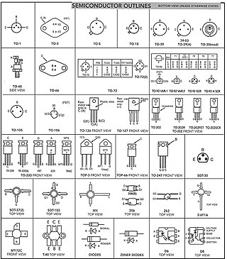
A transistor is a semiconductor device used to amplify or switch electrical signals and power. It is one of the basic building blocks of modern electronics. It is composed of semiconductor material, usually with at least three terminals for connection to an electronic circuit. A voltage or current applied to one pair of the transistor's terminals controls the current through another pair of terminals. Because the controlled (output) power can be higher than the controlling (input) power, a transistor can amplify a signal. Some transistors are packaged individually, but many more in miniature form are found embedded in integrated circuits. Because transistors are the key active components in practically all modern electronics, many people consider them one of the 20th century's greatest inventions.

Digital electronics is a field of electronics involving the study of digital signals and the engineering of devices that use or produce them. This is in contrast to analog electronics which work primarily with analog signals. Despite the name, digital electronics designs includes important analog design considerations.

A semiconductor device is an electronic component that relies on the electronic properties of a semiconductor material for its function. Its conductivity lies between conductors and insulators. Semiconductor devices have replaced vacuum tubes in most applications. They conduct electric current in the solid state, rather than as free electrons across a vacuum or as free electrons and ions through an ionized gas.

In electronics, the metal–oxide–semiconductor field-effect transistor is a type of field-effect transistor (FET), most commonly fabricated by the controlled oxidation of silicon. It has an insulated gate, the voltage of which determines the conductivity of the device. This ability to change conductivity with the amount of applied voltage can be used for amplifying or switching electronic signals. The term metal–insulator–semiconductor field-effect transistor (MISFET) is almost synonymous with MOSFET. Another near-synonym is insulated-gate field-effect transistor (IGFET).

Electromagnetic compatibility (EMC) is the ability of electrical equipment and systems to function acceptably in their electromagnetic environment, by limiting the unintentional generation, propagation and reception of electromagnetic energy which may cause unwanted effects such as electromagnetic interference (EMI) or even physical damage to operational equipment. The goal of EMC is the correct operation of different equipment in a common electromagnetic environment. It is also the name given to the associated branch of electrical engineering.

A bipolar junction transistor (BJT) is a type of transistor that uses both electrons and electron holes as charge carriers. In contrast, a unipolar transistor, such as a field-effect transistor (FET), uses only one kind of charge carrier. A bipolar transistor allows a small current injected at one of its terminals to control a much larger current flowing between the terminals, making the device capable of amplification or switching.

An EPROM, or erasable programmable read-only memory, is a type of programmable read-only memory (PROM) chip that retains its data when its power supply is switched off. Computer memory that can retrieve stored data after a power supply has been turned off and back on is called non-volatile. It is an array of floating-gate transistors individually programmed by an electronic device that supplies higher voltages than those normally used in digital circuits. Once programmed, an EPROM can be erased by exposing it to strong ultraviolet (UV) light source. EPROMs are easily recognizable by the transparent fused quartz window on the top of the package, through which the silicon chip is visible, and which permits exposure to ultraviolet light during erasing.

Electronic test equipment is used to create signals and capture responses from electronic devices under test (DUTs). In this way, the proper operation of the DUT can be proven or faults in the device can be traced. Use of electronic test equipment is essential to any serious work on electronics systems.
This is an index of articles relating to electronics and electricity or natural electricity and things that run on electricity and things that use or conduct electricity.

Automatic test equipment or automated test equipment (ATE) is any apparatus that performs tests on a device, known as the device under test (DUT), equipment under test (EUT) or unit under test (UUT), using automation to quickly perform measurements and evaluate the test results. An ATE can be a simple computer-controlled digital multimeter, or a complicated system containing dozens of complex test instruments capable of automatically testing and diagnosing faults in sophisticated electronic packaged parts or on wafer testing, including system on chips and integrated circuits.

An electronic component is any basic discrete electronic device or physical entity part of an electronic system used to affect electrons or their associated fields. Electronic components are mostly industrial products, available in a singular form and are not to be confused with electrical elements, which are conceptual abstractions representing idealized electronic components and elements. A datasheet for an electronic component is a technical document that provides detailed information about the component's specifications, characteristics, and performance.

An RF switch or microwave switch is a device to route high frequency signals through transmission paths. RF and microwave switches are used extensively in microwave test systems for signal routing between instruments and devices under test (DUT). Incorporating a switch into a switch matrix system enables you to route signals from multiple instruments to single or multiple DUTs. This allows multiple tests to be performed with the same setup, eliminating the need for frequent connects and disconnects. The entire testing process can be automated, increasing the throughput in high-volume production environments.

An image sensor or imager is a sensor that detects and conveys information used to form an image. It does so by converting the variable attenuation of light waves into signals, small bursts of current that convey the information. The waves can be light or other electromagnetic radiation. Image sensors are used in electronic imaging devices of both analog and digital types, which include digital cameras, camera modules, camera phones, optical mouse devices, medical imaging equipment, night vision equipment such as thermal imaging devices, radar, sonar, and others. As technology changes, electronic and digital imaging tends to replace chemical and analog imaging.

A curve tracer is a specialised piece of electronic test equipment used to analyze the characteristics of discrete electronic components, such as diodes, transistors, thyristors, and vacuum tubes. The device contains voltage and current sources that can be used to stimulate the device under test (DUT).
The electron beam prober is a specialized adaption of a standard scanning electron microscope (SEM) that is used for semiconductor failure analysis. While a conventional SEM may be operated in a voltage range of 10–30 keV, the e-beam Prober typically operates at 1 keV. The e-beam prober is capable of measuring voltage and timing waveforms on internal semiconductor signal structures. Waveforms may be measured on metal line, polysilicon and diffusion structures that have an electrically active, changing signal. The operation of the prober is similar to that of a sampling oscilloscope. A continuously looping, repeating test pattern must be applied to the device-under-test (DUT). E-beam probers are used primarily for front side semiconductor analysis. With the advent of flip-chip technology, many e-beam probers have been replaced with back side analysis instruments.
This is the history of the transistor. A transistor is a semiconductor device with at least three terminals for connection to an electric circuit. In the common case, the third terminal controls the flow of current between the other two terminals. This can be used for amplification, as in the case of a radio receiver, or for rapid switching, as in the case of digital circuits.
A Hardware Trojan (HT) is a malicious modification of the circuitry of an integrated circuit. A hardware Trojan is completely characterized by its physical representation and its behavior. The payload of an HT is the entire activity that the Trojan executes when it is triggered. In general, Trojans try to bypass or disable the security fence of a system: for example, leaking confidential information by radio emission. HTs also could disable, damage or destroy the entire chip or components of it.
Transistor laser is a semiconductor device that functions as a transistor with an electrical output and an optical output, as opposed to the typical two electrical outputs. This optical output separates it from typical transistors and, because optical signals travel faster than electrical signals, has the potential to speed up computing immensely. Researchers who discovered the transistor laser developed a new model of Kirchhoff's current law to better model the behavior of simultaneous optical and electrical output.

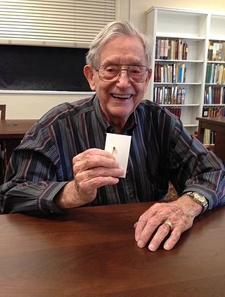
James Robert Biard was an American electrical engineer and inventor who held 73 U.S. patents. Some of his more significant patents include the first infrared light-emitting diode (LED), the optical isolator, Schottky clamped logic circuits, silicon Metal Oxide Semiconductor Read Only Memory, a low bulk leakage current avalanche photodetector, and fiber-optic data links. In 1980, Biard became a member of the staff of Texas A&M University as an Adjunct Professor of Electrical Engineering. In 1991, he was elected as a member into the National Academy of Engineering for contributions to semiconductor light-emitting diodes and lasers, Schotky-clamped logic, and read-only memories.

The field-effect transistor (FET) is a type of transistor that uses an electric field to control the flow of current in a semiconductor. It comes in two types: junction FET (JFET) and metal-oxide-semiconductor FET (MOSFET). FETs have three terminals: source, gate, and drain. FETs control the flow of current by the application of a voltage to the gate, which in turn alters the conductivity between the drain and source.


