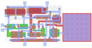
A schematic, or schematic diagram, is a representation of the elements of a system using abstract, graphic symbols rather than realistic pictures. A schematic usually omits all details that are not relevant to the key information the schematic is intended to convey, and may include oversimplified elements in order to make this essential meaning easier to grasp.

An application-specific integrated circuit is an integrated circuit (IC) chip customized for a particular use, rather than intended for general-purpose use. For example, a chip designed to run in a digital voice recorder or a high-efficiency bitcoin miner is an ASIC. Application-specific standard product (ASSP) chips are intermediate between ASICs and industry standard integrated circuits like the 7400 series or the 4000 series. ASIC chips are typically fabricated using metal-oxide-semiconductor (MOS) technology, as MOS integrated circuit chips.
Electronic design automation (EDA), also referred to as electronic computer-aided design (ECAD), is a category of software tools for designing electronic systems such as integrated circuits and printed circuit boards. The tools work together in a design flow that chip designers use to design and analyze entire semiconductor chips. Since a modern semiconductor chip can have billions of components, EDA tools are essential for their design; this article in particular describes EDA specifically with respect to integrated circuits (ICs).

A circuit diagram is a graphical representation of an electrical circuit. A pictorial circuit diagram uses simple images of components, while a schematic diagram shows the components and interconnections of the circuit using standardized symbolic representations. The presentation of the interconnections between circuit components in the schematic diagram does not necessarily correspond to the physical arrangements in the finished device.

Integrated circuit layout, also known IC layout, IC mask layout, or mask design, is the representation of an integrated circuit in terms of planar geometric shapes which correspond to the patterns of metal, oxide, or semiconductor layers that make up the components of the integrated circuit. Originally the overall process was called tapeout as historically early ICs used graphical black crepe tape on mylar media for photo imaging.

GDSII stream format, common acronym GDSII, is a database file format which is the de facto industry standard for data exchange of integrated circuit or IC layout artwork. It is a binary file format representing planar geometric shapes, text labels, and other information about the layout in hierarchical form. The data can be used to reconstruct all or part of the artwork to be used in sharing layouts, transferring artwork between different tools, or creating photomasks.
Place and route is a stage in the design of printed circuit boards, integrated circuits, and field-programmable gate arrays. As implied by the name, it is composed of two steps, placement and routing. The first step, placement, involves deciding where to place all electronic components, circuitry, and logic elements in a generally limited amount of space. This is followed by routing, which decides the exact design of all the wires needed to connect the placed components. This step must implement all the desired connections while following the rules and limitations of the manufacturing process.

In semiconductor design, standard cell methodology is a method of designing application-specific integrated circuits (ASICs) with mostly digital-logic features. Standard cell methodology is an example of design abstraction, whereby a low-level very-large-scale integration (VLSI) layout is encapsulated into an abstract logic representation. Cell-based methodology — the general class to which standard cells belong — makes it possible for one designer to focus on the high-level aspect of digital design, while another designer focuses on the implementation (physical) aspect. Along with semiconductor manufacturing advances, standard cell methodology has helped designers scale ASICs from comparatively simple single-function ICs, to complex multi-million gate system-on-a-chip (SoC) devices.
Standard Parasitic Exchange Format (SPEF) is an IEEE standard for representing parasitic data of wires in a chip in ASCII format. Non-ideal wires have parasitic resistance and capacitance that are captured by SPEF. These wires also have inductance that is not included in SPEF. SPEF is used for delay calculation and ensuring signal integrity of a chip which eventually determines its speed of operation.

OrCAD Systems Corporation was a software company that made OrCAD, a proprietary software tool suite used primarily for electronic design automation (EDA). The software is used mainly by electronic design engineers and electronic technicians to create electronic schematics, perform mixed-signal simulation and electronic prints for manufacturing printed circuit boards. OrCAD was taken over by Cadence Design Systems in 1999 and was integrated with Cadence Allegro since 2005.

Integrated circuit design, or IC design, is a subset of electronics engineering, encompassing the particular logic and circuit design techniques required to design integrated circuits, or ICs. ICs consist of miniaturized electronic components built into an electrical network on a monolithic semiconductor substrate by photolithography.
The electric circuit extraction or simply circuit extraction, also netlist extraction, is the translation of an integrated circuit layout back into the electrical circuit (netlist) it is intended to represent. This extracted circuit is needed for various purposes including circuit simulation, static timing analysis, signal integrity, power analysis and optimization, and logic to layout comparison. Each of these functions require a slightly different representation of the circuit, resulting in the need for multiple layout extractions. In addition, there may be a postprocessing step of converting the device-level circuit into a purely digital circuit, but this is not considered part of the extraction process.
An EDA database is a database specialized for the purpose of electronic design automation. These application specific databases are required because general purpose databases have historically not provided enough performance for EDA applications.

The Electric VLSI Design System is an EDA tool written in the early 1980s by Steven M. Rubin. Electric is used to draw schematics and to do integrated circuit layout. It can also handle hardware description languages such as VHDL and Verilog. The system has many analysis and synthesis tools, including Design rule checking, Simulation, Routing, Layout vs. Schematic, Logical Effort, and more.
CR-5000 is Zuken's design suite for electronics systems and printed circuit boards aimed at the enterprise market. It was developed to tackle complex design needs that involve managing the complete development and manufacturing preparation process on an enterprise-wide scale. CR-5000 offers relevant functionality for the design of complex and high-speed boards, addressing design challenges such as signal integrity and electromagnetic compatibility.

In integrated circuit design, physical design is a step in the standard design cycle which follows after the circuit design. At this step, circuit representations of the components of the design are converted into geometric representations of shapes which, when manufactured in the corresponding layers of materials, will ensure the required functioning of the components. This geometric representation is called integrated circuit layout. This step is usually split into several sub-steps, which include both design and verification and validation of the layout.
A process design kit (PDK) is a set of files used within the semiconductor industry to model a fabrication process for the design tools used to design an integrated circuit. The PDK is created by the foundry defining a certain technology variation for their processes. It is then passed to their customers to use in the design process. The customers may enhance the PDK, tailoring it to their specific design styles and markets. The designers use the PDK to design, simulate, draw and verify the design before handing the design back to the foundry to produce chips. The data in the PDK is specific to the foundry's process variation and is chosen early in the design process, influenced by the market requirements for the chip. An accurate PDK will increase the chances of first-pass successful silicon.
In the automated design of integrated circuits, signoff checks is the collective name given to a series of verification steps that the design must pass before it can be taped out. This implies an iterative process involving incremental fixes across the board using one or more check types, and then retesting the design. There are two types of sign-off's: front-end sign-off and back-end sign-off. After back-end sign-off the chip goes to fabrication. After listing out all the features in the specification, the verification engineer will write coverage for those features to identify bugs, and send back the RTL design to the designer. Bugs, or defects, can include issues like missing features, errors in design, etc. When the coverage reaches a maximum% then the verification team will sign it off. By using a methodology like UVM, OVM, or VMM, the verification team develops a reusable environment. Nowadays, UVM is more popular than others.
In electronic design automation, parasitic extraction is the calculation of the parasitic effects in both the designed devices and the required wiring interconnects of an electronic circuit: parasitic capacitances, parasitic resistances and parasitic inductances, commonly called parasitic devices, parasitic components, or simply parasitics.
Library Exchange Format (LEF) is a specification for representing the physical layout of an integrated circuit in an ASCII format. It includes design rules and abstract information about the cells.


