This article may be too technical for most readers to understand.(June 2020) |
AArch64 or ARM64 is the 64-bit extension of the ARM architecture family. It was first introduced with the Armv8-A architecture, and had many extension updates. [1]
This article may be too technical for most readers to understand.(June 2020) |
AArch64 or ARM64 is the 64-bit extension of the ARM architecture family. It was first introduced with the Armv8-A architecture, and had many extension updates. [1]
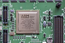
Announced in October 2011, [2] ARMv8-A represents a fundamental change to the ARM architecture. It adds an optional 64-bit architecture, named "AArch64", and the associated new "A64" instruction set. AArch64 provides user-space compatibility with the existing 32-bit architecture ("AArch32" / ARMv7-A), and instruction set ("A32"). The 16-32bit Thumb instruction set is referred to as "T32" and has no 64-bit counterpart. ARMv8-A allows 32-bit applications to be executed in a 64-bit OS, and a 32-bit OS to be under the control of a 64-bit hypervisor. [3] ARM announced their Cortex-A53 and Cortex-A57 cores on 30 October 2012. [4] Apple was the first to release an ARMv8-A compatible core (Cyclone) in a consumer product (iPhone 5S). AppliedMicro, using an FPGA, was the first to demo ARMv8-A. [5] The first ARMv8-A SoC from Samsung is the Exynos 5433 used in the Galaxy Note 4, which features two clusters of four Cortex-A57 and Cortex-A53 cores in a big.LITTLE configuration; but it will run only in AArch32 mode. [6]
ARMv8-A includes the VFPv3/v4 and advanced SIMD (Neon) as standard features in both AArch32 and AArch64. It also adds cryptography instructions supporting AES, SHA-1/SHA-256 and finite field arithmetic. [7]
Extension: Data gathering hint (ARMv8.0-DGH).
AArch64 was introduced in ARMv8-A and is included in subsequent versions of ARMv8-A. It was also introduced in ARMv8-R as an option, after its introduction in ARMv8-A; it is not included in ARMv8-M.
The main opcode for selecting which group an A64 instruction belongs to is at bits 25-28.
| Type | Bit | |||||||||||||||||||||||||||||||
|---|---|---|---|---|---|---|---|---|---|---|---|---|---|---|---|---|---|---|---|---|---|---|---|---|---|---|---|---|---|---|---|---|
| 31 | 30 | 29 | 28 | 27 | 26 | 25 | 24 | 23 | 22 | 21 | 20 | 19 | 18 | 17 | 16 | 15 | 14 | 13 | 12 | 11 | 10 | 9 | 8 | 7 | 6 | 5 | 4 | 3 | 2 | 1 | 0 | |
| Reserved | 0 | op0 | 0 | 0 | 0 | 0 | op1 | |||||||||||||||||||||||||
| SME | 1 | op0 | 0 | 0 | 0 | 0 | Varies | |||||||||||||||||||||||||
| Unallocated | 0 | 0 | 0 | 1 | ||||||||||||||||||||||||||||
| SVE | 0 | 0 | 1 | 0 | Varies | |||||||||||||||||||||||||||
| Unallocated | 0 | 0 | 1 | 1 | ||||||||||||||||||||||||||||
| Data Processing — Immediate PC-rel. | op | immlo | 1 | 0 | 0 | 0 | 0 | immhi | Rd | |||||||||||||||||||||||
| Data Processing — Immediate Others | sf | 1 | 0 | 0 | 01-11 | Rd | ||||||||||||||||||||||||||
| Branches + System Instructions | op0 | 1 | 0 | 1 | op1 | op2 | ||||||||||||||||||||||||||
| Load and Store Instructions | op0 | 1 | op1 | 0 | op2 | op3 | op4 | |||||||||||||||||||||||||
| Data Processing — Register | sf | op0 | op1 | 1 | 0 | 1 | op2 | op3 | ||||||||||||||||||||||||
| Data Processing — Floating Point and SIMD | op0 | 1 | 1 | 1 | op1 | op2 | op3 | |||||||||||||||||||||||||
In December 2014, ARMv8.1-A, [9] an update with "incremental benefits over v8.0", was announced. The enhancements fell into two categories: changes to the instruction set, and changes to the exception model and memory translation.
Instruction set enhancements included the following:
Enhancements for the exception model and memory translation system included the following:
In January 2016, ARMv8.2-A was announced. [11] Its enhancements fell into four categories:
The Scalable Vector Extension (SVE) is "an optional extension to the ARMv8.2-A architecture and newer" developed specifically for vectorization of high-performance computing scientific workloads. [12] [13] The specification allows for variable vector lengths to be implemented from 128 to 2048 bits. The extension is complementary to, and does not replace, the NEON extensions.
A 512-bit SVE variant has already been implemented on the Fugaku supercomputer using the Fujitsu A64FX ARM processor; this computer [14] was the fastest supercomputer in the world for two years, from June 2020 [15] to May 2022. [16] A more flexible version, 2x256 SVE, was implemented by the AWS Graviton3 ARM processor.
SVE is supported by the GCC compiler, with GCC 8 supporting automatic vectorization [13] and GCC 10 supporting C intrinsics. As of July 2020 [update] , LLVM and clang support C and IR intrinsics. ARM's own fork of LLVM supports auto-vectorization. [17]
In October 2016, ARMv8.3-A was announced. Its enhancements fell into six categories: [18]
ARMv8.3-A architecture is now supported by (at least) the GCC 7 compiler. [22]
In November 2017, ARMv8.4-A was announced. Its enhancements fell into these categories: [23] [24] [25]
In September 2018, ARMv8.5-A was announced. Its enhancements fell into these categories: [26] [27] [28]
On 2 August 2019, Google announced Android would adopt Memory Tagging Extension (MTE). [30]
In March 2021, ARMv9-A was announced. ARMv9-A's baseline is all the features from ARMv8.5. [31] [32] [33] ARMv9-A also adds:
In September 2019, ARMv8.6-A was announced. Its enhancements fell into these categories: [26] [38]
For example, fine-grained traps, Wait-for-Event (WFE) instructions, EnhancedPAC2 and FPAC. The bfloat16 extensions for SVE and Neon are mainly for deep learning use. [40]
In September 2020, ARMv8.7-A was announced. Its enhancements fell into these categories: [26] [41]
In September 2021, ARMv8.8-A and ARMv9.3-A were announced. Their enhancements fell into these categories: [26] [43]
In September 2022, ARMv8.9-A and ARMv9.4-A were announced, including: [45]
This section needs expansionwith: examples and additional citations. You can help by adding to it.(May 2021) |
Optional AArch64 support was added to the Armv8-R profile, with the first Arm core implementing it being the Cortex-R82. [46] It adds the A64 instruction set, with some changes to the memory barrier instructions. [47]

Single instruction, multiple data (SIMD) is a type of parallel processing in Flynn's taxonomy. SIMD can be internal and it can be directly accessible through an instruction set architecture (ISA), but it should not be confused with an ISA. SIMD describes computers with multiple processing elements that perform the same operation on multiple data points simultaneously.
ARM is a family of RISC instruction set architectures (ISAs) for computer processors. Arm Ltd. develops the ISAs and licenses them to other companies, who build the physical devices that use the instruction set. It also designs and licenses cores that implement these ISAs.

In computer architecture, 64-bit integers, memory addresses, or other data units are those that are 64 bits wide. Also, 64-bit central processing units (CPU) and arithmetic logic units (ALU) are those that are based on processor registers, address buses, or data buses of that size. A computer that uses such a processor is a 64-bit computer.
In computer architecture, 128-bit integers, memory addresses, or other data units are those that are 128 bits wide. Also, 128-bit central processing unit (CPU) and arithmetic logic unit (ALU) architectures are those that are based on registers, address buses, or data buses of that size.
In C and related programming languages, long double refers to a floating-point data type that is often more precise than double precision though the language standard only requires it to be at least as precise as double. As with C's other floating-point types, it may not necessarily map to an IEEE format.
Advanced Vector Extensions are SIMD extensions to the x86 instruction set architecture for microprocessors from Intel and Advanced Micro Devices (AMD). They were proposed by Intel in March 2008 and first supported by Intel with the Sandy Bridge processor shipping in Q1 2011 and later by AMD with the Bulldozer processor shipping in Q3 2011. AVX provides new features, new instructions, and a new coding scheme.
An AES instruction set is a set of instructions that are specifically designed to perform AES encryption and decryption operations efficiently. These instructions are typically found in modern processors and can greatly accelerate AES operations compared to software implementations. An AES instruction set includes instructions for key expansion, encryption, and decryption using various key sizes.

The ARM Cortex-M is a group of 32-bit RISC ARM processor cores licensed by ARM Limited. These cores are optimized for low-cost and energy-efficient integrated circuits, which have been embedded in tens of billions of consumer devices. Though they are most often the main component of microcontroller chips, sometimes they are embedded inside other types of chips too. The Cortex-M family consists of Cortex-M0, Cortex-M0+, Cortex-M1, Cortex-M3, Cortex-M4, Cortex-M7, Cortex-M23, Cortex-M33, Cortex-M35P, Cortex-M52, Cortex-M55, Cortex-M85. A floating-point unit (FPU) option is available for Cortex-M4 / M7 / M33 / M35P / M52 / M55 / M85 cores, and when included in the silicon these cores are sometimes known as "Cortex-MxF", where 'x' is the core variant.
The ARM Cortex-A is a group of 32-bit and 64-bit RISC ARM processor cores licensed by Arm Holdings. The cores are intended for application use. The group consists of 32-bit only cores: ARM Cortex-A5, ARM Cortex-A7, ARM Cortex-A8, ARM Cortex-A9, ARM Cortex-A12, ARM Cortex-A15, ARM Cortex-A17 MPCore, and ARM Cortex-A32, 32/64-bit mixed operation cores: ARM Cortex-A35, ARM Cortex-A53, ARM Cortex-A55, ARM Cortex-A57, ARM Cortex-A72, ARM Cortex-A73, ARM Cortex-A75, ARM Cortex-A76, ARM Cortex-A77, ARM Cortex-A78, ARM Cortex-A710, and ARM Cortex-A510 Refresh, and 64-bit only cores: ARM Cortex-A34, ARM Cortex-A65, ARM Cortex-A510 (2021), ARM Cortex-A715, ARM Cortex-A520, and ARM Cortex-A720.
The ARM Cortex-A12 is a 32-bit processor core licensed by ARM Holdings implementing the ARMv7-A architecture. It provides up to 4 cache-coherent cores. The Cortex-A12 is a successor to the Cortex-A9.
The ARM Cortex-A57 is a central processing unit implementing the ARMv8-A 64-bit instruction set designed by ARM Holdings. The Cortex-A57 is an out-of-order superscalar pipeline. It is available as SIP core to licensees, and its design makes it suitable for integration with other SIP cores into one die constituting a system on a chip (SoC).
The ARM Cortex-A17 is a 32-bit processor core implementing the ARMv7-A architecture, licensed by ARM Holdings. Providing up to four cache-coherent cores, it serves as the successor to the Cortex-A9 and replaces the previous ARM Cortex-A12 specifications. ARM claims that the Cortex-A17 core provides 60% higher performance than the Cortex-A9 core, while reducing the power consumption by 20% under the same workload.

The ARM Cortex-A53 is one of the first two central processing units implementing the ARMv8-A 64-bit instruction set designed by ARM Holdings' Cambridge design centre, along with the Cortex-A57. The Cortex-A53 is a 2-wide decode superscalar processor, capable of dual-issuing some instructions. It was announced October 30, 2012 and is marketed by ARM as either a stand-alone, more energy-efficient alternative to the more powerful Cortex-A57 microarchitecture, or to be used alongside a more powerful microarchitecture in a big.LITTLE configuration. It is available as an IP core to licensees, like other ARM intellectual property and processor designs.
This is a comparison of ARM instruction set architecture application processor cores designed by ARM Holdings and 3rd parties. It does not include ARM Cortex-R, ARM Cortex-M, or legacy ARM cores.
The ARM Cortex-A72 is a central processing unit implementing the ARMv8-A 64-bit instruction set designed by ARM Holdings' Austin design centre. The Cortex-A72 is a 3-way decode out-of-order superscalar pipeline. It is available as SIP core to licensees, and its design makes it suitable for integration with other SIP cores into one die constituting a system on a chip (SoC). The Cortex-A72 was announced in 2015 to serve as the successor of the Cortex-A57, and was designed to use 20% less power or offer 90% greater performance.

Power ISA is a reduced instruction set computer (RISC) instruction set architecture (ISA) currently developed by the OpenPOWER Foundation, led by IBM. It was originally developed by IBM and the now-defunct Power.org industry group. Power ISA is an evolution of the PowerPC ISA, created by the mergers of the core PowerPC ISA and the optional Book E for embedded applications. The merger of these two components in 2006 was led by Power.org founders IBM and Freescale Semiconductor.
Permute instructions, part of bit manipulation as well as vector processing, copy unaltered contents from a source array to a destination array, where the indices are specified by a second source array. The size (bitwidth) of the source elements is not restricted but remains the same as the destination size.
The ARM Cortex-A710 is the successor to the ARM Cortex-A78, being the First-Generation Armv9 “big” Cortex CPU. It is the companion to the ARM Cortex-A510 "LITTLE" efficiency core. It was designed by ARM Ltd.'s Austin centre. It is the fourth and last iteration of Arm’s Austin core family. It forms part of Arm's Total Compute Solutions 2021 (TCS21) along with Arm's Cortex-X2, Cortex-A510, Mali-G710 and CoreLink CI-700/NI-700.
The ARM Cortex-X2 is a central processing unit implementing the ARMv9-A 64-bit instruction set designed by ARM Holdings' Austin design centre as part of ARM's Cortex-X Custom (CXC) program. It forms part of Arm's Total Compute Solutions 2021 (TCS21) along with Arm's Cortex-A710, Cortex-A510, Mali-G710 and CoreLink CI-700/NI-700.
The ARM Neoverse is a group of 64-bit ARM processor cores licensed by Arm Holdings. The cores are intended for datacenter, edge computing, and high-performance computing use. The group consists of ARM Neoverse V-Series, ARM Neoverse N-Series, and ARM Neoverse E-Series.
pointer authentication extension is defined to be mandatory extension on ARMv8.3-A and is not optional
The ARMv8.3-A architecture is now supported. It can be used by specifying the -march=armv8.3-a option. [..] The option -msign-return-address= is supported to enable return address protection using ARMv8.3-A Pointer Authentication Extensions.