
Advanced Micro Devices, Inc., commonly abbreviated as AMD, is an American multinational semiconductor company based in Santa Clara, California, that develops computer processors and related technologies for business and consumer markets.

The southbridge is one of the two chips in the core logic chipset on a personal computer (PC) motherboard, the other being the northbridge. The southbridge typically implements the slower capabilities of the motherboard in a northbridge/southbridge chipset computer architecture. In systems with Intel chipsets, the southbridge is named I/O Controller Hub (ICH), while AMD has named its southbridge Fusion Controller Hub (FCH) since the introduction of its Fusion Accelerated Processing Unit (APU) while moving the functions of the Northbridge onto the CPU die, hence making it similar in function to the Platform hub controller.

coreboot, formerly known as LinuxBIOS, is a software project aimed at replacing proprietary firmware found in most computers with a lightweight firmware designed to perform only the minimum number of tasks necessary to load and run a modern 32-bit or 64-bit operating system.

AMD Accelerated Processing Unit (APU), formerly known as Fusion, is a series of 64-bit microprocessors from Advanced Micro Devices (AMD), combining a general-purpose AMD64 central processing unit (CPU) and 3D integrated graphics processing unit (IGPU) on a single die.
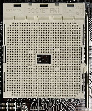
Socket FM1 is a CPU socket for desktop computers used by AMD early A-series APUs ("Llano") processors and Llano-derived Athlon II processors. It was released in July 2011. Its direct successors are Socket FM2 and Socket FM2+, while Socket AM1 is targeting low-power SoCs.

Socket FM2 is a CPU socket used by AMD's desktop Trinity and Richland APUs to connect to the motherboard as well as Athlon X2 and Athlon X4 processors based on them. FM2 was launched on September 27, 2012. Motherboards which feature the at the time new FM2 CPU socket also utilize AMD's at the time new A85X chipset.
Socket FM2+ is a zero insertion force CPU socket designed by AMD for their desktop "Kaveri" APUs (Steamroller-based) and Godavari APUs (Steamroller-based) to connect to the motherboard. The FM2+ has a slightly different pin configuration to Socket FM2 with two additional pin sockets. Socket FM2+ APUs are not compatible with Socket FM2 motherboards due to the aforementioned additional pins. However, socket FM2 APUs such as "Richland" and "Trinity" are compatible with the FM2+ socket.
The Socket FT1 or BGA413 is a CPU socket released in January 2011 from AMD for its APUs codenamed Desna, Ontario, Zacate and Hondo. The uber name is "Brazos".

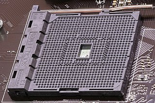
Socket AM4 is a PGA microprocessor socket used by AMD's central processing units (CPUs) built on the Zen and Excavator microarchitectures.

Zen 2 is a computer processor microarchitecture by AMD. It is the successor of AMD's Zen and Zen+ microarchitectures, and is fabricated on the 7 nm MOSFET node from TSMC. The microarchitecture powers the third generation of Ryzen processors, known as Ryzen 3000 for the mainstream desktop chips, Ryzen 4000U/H and Ryzen 5000U for mobile applications, as Threadripper 3000 for high-end desktop systems, and as Ryzen 4000G for accelerated processing units (APUs). The Ryzen 3000 series CPUs were released on 7 July 2019, while the Zen 2-based Epyc server CPUs were released on 7 August 2019. An additional chip, the Ryzen 9 3950X, was released in November 2019.
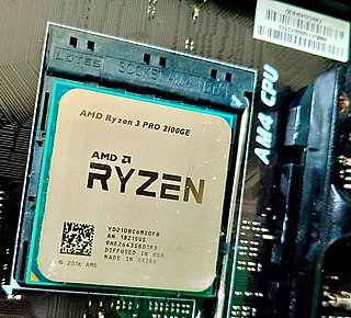
Ryzen is a brand of multi-core x86-64 microprocessors designed and marketed by AMD for desktop, mobile, server, and embedded platforms based on the Zen microarchitecture. It consists of central processing units (CPUs) marketed for mainstream, enthusiast, server, and workstation segments and accelerated processing units (APUs) marketed for mainstream and entry-level segments and embedded systems applications.

Socket TR4, also known as Socket SP3r2, is a zero insertion force land grid array (LGA) CPU socket designed by AMD supporting its first- and second-generation Zen-based Ryzen Threadripper desktop processors, launched on August 10, 2017 for the high-end desktop and workstation platforms. It was succeeded by Socket sTRX4 for the third generation of Ryzen Threadripper processors.

Zen 4 is the codename for a CPU microarchitecture designed by AMD, released on September 27, 2022. It is the successor to Zen 3 and uses TSMC's N5 process for CCDs. Zen 4 powers Ryzen 7000 mainstream desktop processors and will be used in high-end mobile processors, thin & light mobile processors, as well as EPYC 9004 server processors.
Socket sTRX4, also known as Socket SP3r3, is a land grid array (LGA) CPU socket designed by AMD supporting its Zen 2-based third-generation Ryzen Threadripper desktop processors, launched on November 25, 2019 for the high-end desktop and workstation platforms.

Zen 3 is the codename for a CPU microarchitecture by AMD, released on November 5, 2020. It is the successor to Zen 2 and uses TSMC's 7 nm process for the chiplets and GlobalFoundries's 14 nm process for the I/O die on the server chips and 12 nm for desktop chips. Zen 3 powers Ryzen 5000 mainstream desktop processors and Epyc server processors. Zen 3 is supported on motherboards with 500 series chipsets; 400 series boards also saw support on select B450 / X470 motherboards with certain BIOSes. Zen 3 is the last microarchitecture before AMD switched to DDR5 memory and new sockets, which are AM5 for the desktop "Ryzen" chips alongside SP5 and SP6 for the EPYC server platform. According to AMD, Zen 3 has a 19% higher instructions per cycle (IPC) on average than Zen 2.

Socket AM5 is a zero insertion force flip-chip land grid array (LGA) CPU socket designed by Advanced Micro Devices, that is used for AMD Ryzen microprocessors starting with the Zen 4 microarchitecture. AM5 replaces the Socket AM4 and is AMD's first LGA socket designed for mainstream, non-enthusiast CPUs.