
Electroluminescence (EL) is an optical phenomenon and electrical phenomenon in which a material emits light in response to the passage of an electric current or to a strong electric field. This is distinct from black body light emission resulting from heat (incandescence), a chemical reaction (chemiluminescence), sound (sonoluminescence), or other mechanical action (mechanoluminescence).
A flat-panel display (FPD) is an electronic display device used to enable people to see content in a range of entertainment, consumer electronics, personal computer, and mobile devices, and many types of medical, transportation and industrial equipment. Such panels, or screens, are far lighter and thinner than traditional cathode ray tube (CRT) television sets and are usually less than 10 centimetres (3.9 in) thick. Flat-panel displays can be divided into two display device categories: volatile and static. Volatile displays require that pixels be periodically electronically refreshed to retain their state. A volatile display only shows an image when it has battery or AC mains power. Static flat-panel displays rely on materials whose color states are bistable, and as such, flat-panel displays retain the text or images on the screen even when the power is off. As of 2016, flat-panel displays have almost completely replaced old CRT displays. In many 2010-era applications, specifically small portable devices such as laptops, mobile phones, smartphones, digital cameras, camcorders, point-and-shoot cameras, and pocket video cameras, any display disadvantages of flat-panels are made up for by portability advantages.
Indium tin oxide (ITO) is a ternary composition of indium, tin and oxygen in varying proportions. Depending on the oxygen content, it can be described as either a ceramic or an alloy. Indium tin oxide is typically encountered as an oxygen-saturated composition with a formulation of 74% In, 18% Sn, and 8% O by weight. Oxygen-saturated compositions are so typical that unsaturated compositions are termed oxygen-deficient ITO. It is transparent and colorless in thin layers, while in bulk form it is yellowish to gray. In the infrared region of the spectrum it acts as a metal-like mirror.
Applied Materials, Inc. is an American corporation that supplies equipment, services and software for the manufacture of semiconductor chips for electronics, flat panel displays for computers, smartphones, televisions, and solar products. Integral to the growth of Silicon Valley, the company also supplies equipment to produce coatings for flexible electronics, packaging and other applications. The company is headquartered in Santa Clara, California.

Lamination is the technique/process of manufacturing a material in multiple layers, so that the composite material achieves improved strength, stability, sound insulation, appearance, or other properties from the use of the differing materials, such as plastic. A laminate is a permanently assembled object created using heat, pressure, welding, or adhesives. Various coating machines, machine presses and calendering equipment are used.
A thin film is a layer of material ranging from fractions of a nanometer (monolayer) to several micrometers in thickness. The controlled synthesis of materials as thin films is a fundamental step in many applications. A familiar example is the household mirror, which typically has a thin metal coating on the back of a sheet of glass to form a reflective interface. The process of silvering was once commonly used to produce mirrors, while more recently the metal layer is deposited using techniques such as sputtering. Advances in thin film deposition techniques during the 20th century have enabled a wide range of technological breakthroughs in areas such as magnetic recording media, electronic semiconductor devices, Integrated passive devices, LEDs, optical coatings, hard coatings on cutting tools, and for both energy generation and storage. It is also being applied to pharmaceuticals, via thin-film drug delivery. A stack of thin films is called a multilayer.

Metallizing is the general name for the technique of coating metal on the surface of objects. Metallic coatings may be decorative, protective or functional.

A surface-conduction electron-emitter display (SED) is a display technology for flat panel displays developed by a number of companies. SEDs use nanoscopic-scale electron emitters to energize colored phosphors and produce an image. In a general sense, an SED consists of a matrix of tiny cathode ray tubes, each "tube" forming a single sub-pixel on the screen, grouped in threes to form red-green-blue (RGB) pixels. SEDs combine the advantages of CRTs, namely their high contrast ratios, wide viewing angles and very fast response times, with the packaging advantages of LCD and other flat panel displays. They also use much less power than an LCD television of the same size.
A coating is a covering that is applied to the surface of an object, usually referred to as the substrate. The purpose of applying the coating may be decorative, functional, or both.
Low emissivity refers to a surface condition that emits low levels of radiant thermal (heat) energy. All materials absorb, reflect, and emit radiant energy according to Planck's law but here, the primary concern is a special wavelength interval of radiant energy, namely thermal radiation of materials. In common use, especially building applications, the temperature range of approximately -40 to +80 degrees Celsius is the focus, but in aerospace and industrial process engineering, much broader ranges are of practical concern.

Ion plating (IP) is a physical vapor deposition (PVD) process that is sometimes called ion assisted deposition (IAD) or ion vapor deposition (IVD) and is a version of vacuum deposition. Ion plating uses concurrent or periodic bombardment of the substrate, and deposits film by atomic-sized energetic particles. Bombardment prior to deposition is used to sputter clean the substrate surface. During deposition the bombardment is used to modify and control the properties of the depositing film. It is important that the bombardment be continuous between the cleaning and the deposition portions of the process to maintain an atomically clean interface.

Electroluminescent Displays (ELDs) are a type of flat panel display created by sandwiching a layer of electroluminescent material such as GaAs between two layers of conductors. When current flows, the layer of material emits radiation in the form of visible light. Electroluminescence (EL) is an optical and electrical phenomenon where a material emits light in response to an electric current passed through it, or to a strong electric field. The term "electroluminescent display" describes displays that use neither LED nor OLED devices, that instead use traditional electroluminescent materials. Beneq is the only manufacturer of TFEL and TAESL displays, which are branded as LUMINEQ Displays. The structure of a TFEL is similar to that of a passive matrix LCD or OLED display, and TAESL displays are essentially transparent TEFL displays with transparent electrodes. TAESL displays can have a transparency of 80%. Both TEFL and TAESL displays use chip-on-glass technology, which mounts the display driver IC directly on one of the edges of the display. TAESL displays can be embedded onto glass sheets. Unlike LCDs, TFELs are much more rugged and can operate at temperatures from −60 to 105 °C and unlike OLEDs, TFELs can operate for 100,000 hours without considerable burn-in, only losing about 80% of its initial brightness. The electroluminescent material is deposited using atomic layer deposition, which is a process that deposits one 1-atom thick layer at a time.

Tantalum nitride (TaN) is a chemical compound, a nitride of tantalum. There are multiple phases of compounds, stoichimetrically from Ta2N to Ta3N5, including TaN.
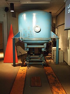
Vacuum deposition is a group of processes used to deposit layers of material atom-by-atom or molecule-by-molecule on a solid surface. These processes operate at pressures well below atmospheric pressure. The deposited layers can range from a thickness of one atom up to millimeters, forming freestanding structures. Multiple layers of different materials can be used, for example to form optical coatings. The process can be qualified based on the vapor source; physical vapor deposition uses a liquid or solid source and chemical vapor deposition uses a chemical vapor.
Physical vapor deposition (PVD), sometimes called physical vapor transport (PVT), describes a variety of vacuum deposition methods which can be used to produce thin films and coatings. PVD is characterized by a process in which the material goes from a condensed phase to a vapor phase and then back to a thin film condensed phase. The most common PVD processes are sputtering and evaporation. PVD is used in the manufacture of items which require thin films for mechanical, optical, chemical or electronic functions. Examples include semiconductor devices such as thin film solar panels, aluminized PET film for food packaging and balloons, and titanium nitride coated cutting tools for metalworking. Besides PVD tools for fabrication, special smaller tools have been developed.

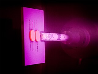
Sputter deposition is a physical vapor deposition (PVD) method of thin film deposition by the phenomenon of sputtering. This involves ejecting material from a "target" that is a source onto a "substrate" such as a silicon wafer. Resputtering is re-emission of the deposited material during the deposition process by ion or atom bombardment. Sputtered atoms ejected from the target have a wide energy distribution, typically up to tens of eV. The sputtered ions can ballistically fly from the target in straight lines and impact energetically on the substrates or vacuum chamber. Alternatively, at higher gas pressures, the ions collide with the gas atoms that act as a moderator and move diffusively, reaching the substrates or vacuum chamber wall and condensing after undergoing a random walk. The entire range from high-energy ballistic impact to low-energy thermalized motion is accessible by changing the background gas pressure. The sputtering gas is often an inert gas such as argon. For efficient momentum transfer, the atomic weight of the sputtering gas should be close to the atomic weight of the target, so for sputtering light elements neon is preferable, while for heavy elements krypton or xenon are used. Reactive gases can also be used to sputter compounds. The compound can be formed on the target surface, in-flight or on the substrate depending on the process parameters. The availability of many parameters that control sputter deposition make it a complex process, but also allow experts a large degree of control over the growth and microstructure of the film.
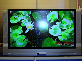
Large-screen television technology developed rapidly in the late 1990s and 2000s. Prior to the development of thin-screen technologies, rear-projection television was standard for larger displays, and jumbotron, a non-projection video display technology, was used at stadiums and concerts. Various thin-screen technologies are being developed, but only liquid crystal display (LCD), plasma display (PDP) and Digital Light Processing (DLP) have been publicly released. Recent technologies like organic light-emitting diode (OLED) as well as not-yet-released technologies like surface-conduction electron-emitter display (SED) or field emission display (FED) are in development to replace earlier flat-screen technologies in picture quality.
High-power impulse magnetron sputtering is a method for physical vapor deposition of thin films which is based on magnetron sputter deposition. HIPIMS utilises extremely high power densities of the order of kW⋅cm−2 in short pulses (impulses) of tens of microseconds at low duty cycle of < 10%. Distinguishing features of HIPIMS are a high degree of ionisation of the sputtered metal and a high rate of molecular gas dissociation which result in high density of deposited films. The ionization and dissociation degree increase according to the peak cathode power. The limit is determined by the transition of the discharge from glow to arc phase. The peak power and the duty cycle are selected so as to maintain an average cathode power similar to conventional sputtering (1–10 W⋅cm−2).
Self-cleaning glass is a specific type of glass with a surface that keeps itself free of dirt and grime.

Transparent conducting films (TCFs) are thin films of optically transparent and electrically conductive material. They are an important component in a number of electronic devices including liquid-crystal displays, OLEDs, touchscreens and photovoltaics. While indium tin oxide (ITO) is the most widely used, alternatives include wider-spectrum transparent conductive oxides (TCOs), conductive polymers, metal grids and random metallic networks, carbon nanotubes (CNT), graphene, nanowire meshes and ultra thin metal films.