Compressed instruction set

Last updated

A compressed instruction set, or simply compressed instructions, are a variation on a microprocessor's instruction set architecture (ISA) that allows instructions to be represented in a more compact format. In most real-world examples, compressed instructions are 16 bits long in a processor that would otherwise use 32-bit instructions. The 16-bit ISA is a subset of the full 32-bit ISA, not a separate instruction set. The smaller format requires some tradeoffs: generally, there are fewer instructions available, and fewer processor registers can be used.

Contents

The concept was originally introduced by Hitachi as a way to improve the code density of their SuperH RISC processor design as it moved from 16-bit to 32-bit instructions in the SH-5 version. The new design had two instruction sets, one giving access to the entire ISA of the new design, and a smaller 16-bit set known as SHcompact that allowed programs to run in smaller amounts of main memory. As the memory of even the smallest systems is now orders of magnitude larger than the systems that spawned the concept, size is no longer the main concern. Today the advantage is that it reduces the number of accesses to main memory and thereby reduces energy use in mobile devices.

Hitachi's patents were licensed by Arm Ltd. for their processors, where it was known as "Thumb". Similar systems are found in MIPS16e and PowerPC VLE. The original patents have expired and the concept can be found in a number of modern designs, including RISC-V, which was designed from the outset to use it. The introduction of 64-bit computing has led to the term no longer being as widely used; these processors generally use 32-bit instructions and are technically a form of compressed ISA, but as they are mostly modified versions of an older ISA from a 32-bit version of the same processor family; there is no real compression.

Concept

Microprocessors encode their instructions as a series of bits, normally divided into a number of 8-bit bytes. For instance, in the MOS 6502, the ADC instruction performs binary addition between an operand value and the value already stored in the accumulator. There are a variety of places the processor might find the operand; it might be located in main memory, or in the special zero page, or be an explicit constant like "10". Each of these variations used a different 8-bit instruction, or opcode; if one wanted to add the constant 10 to the accumulator the instruction would be encoded in memory as $69 $0A, with $0A being hexadecimal for the decimal value 10. If it was instead adding the value stored in main memory at location $4400, it would be $6D $0044, with a little-endian address. [1]

Note that the second instruction requires three bytes because the memory address is 16 bits long. Depending on the instruction, it might use one, two, or three bytes. [1] This is now known as a variable length instruction set, although that term was not common at the time as most processors, including mainframes and minicomputers, normally used some variation of this concept. Even in the late 1970s, as microprocessors began to move from 8-bit formats to 16, this concept remained common; the Intel 8088 continued to use 8-bit opcodes which could be followed by zero to six additional bytes depending on the addressing mode. [2]

It was during the move to 32-bit systems, and especially as the RISC concept began to take over processor design, that variable length instructions began to go away. In the MIPS architecture, for instance, all instructions are a single 32-bit value, with a 6-bit opcode in the most significant bits and the remaining 26 bits used in various ways representing its limited set of addressing modes. Most RISC designs are similar. Moving to a fixed-length instruction format was one of the key design concepts behind the performance of early RISC designs; in earlier systems the instruction might take one to six memory cycles to read, requiring wiring between various parts of the logic to ensure the processor didn't attempt to perform the instruction before the data was ready. In RISC designs, operations normally take one cycle, greatly simplifying the decoding. The savings in these interlocking circuits is instead applied to additional logic or adding processor registers, which have a direct impact on performance. [3]

Code density

The downside to the RISC approach is that many instructions simply do not require four bytes. For instance, the Logical Shift Left instruction shifts the bits in a register to the left. In the 6502, which has only a single arithmetic register A, this instruction can be represented entirely by its 8-bit opcode $06. [1] On processors with more registers, all that is needed is the opcode and register number, another 4 or 5 bits. On MIPS, for instance, the instruction needs only a 6-bit opcode and a 5-bit register number. But as is the case for most RISC designs, the instruction still takes up a full 32 bits. As these sorts of instructions are relatively common, RISC programs generally take up more memory than the same program on a variable length processor. [4]

In the 1980s, when the RISC concept was first emerging, this was a common point of complaint. As the instructions took up more room, the system would have to spend more time reading instructions from memory. It was suggested these extra accesses might actually slow the program down. Extensive benchmarking eventually demonstrated RISC was faster in almost all cases, and this argument faded. However, there are cases where memory use remains a concern regardless of performance, and that is in small systems and embedded applications. Even in the early 2000s, the price of DRAM was enough that cost-sensitive devices had limited memory. It was for this market that Hitachi developed the SuperH design. [5]

In the earlier SuperH designs, SH-1 through SH-4, instructions always take up 16 bits. The resulting instruction set has real-world limitations; for instance, it can only perform two-operand math of the form A = A + B, whereas most processors of the era used the three-operand format, A = B + C. By removing one operand, four bits are removed from the instruction (there are 16 registers, needing 4 bits), although this is at the cost of making math code somewhat more complex to write. For the markets targeted by the SuperH, this was an easy tradeoff to make. A significant advantage of the 16-bit format is that the instruction cache now holds twice as many instructions for any given amount of SRAM. This allows the system to perform at higher speeds, although some of that might be mitigated by the use of additional instructions needed to perform operations that might be performed by a single 3-operand instruction. [6]

For the SH-5, Hitachi moved to a 32-bit instruction format. In order to provide backward compatibility with their earlier designs, they included a second instruction set, SHcompact. SHcompact mapped the original 16-bit instructions one-way onto the internal 32-bit instruction; it did not perform multiple instructions as would be the case in earlier microcoded processors, it was simply a smaller format for the same instruction. This allowed the original small-format programs to be easily ported to the new SH-5, while adding little to the complexity of the instruction decoder. [7]

ARM licensed a number of Hitachi's patents on aspects of the instruction design and used them to implement their Thumb instructions. ARM processors with a "T" in the name included this instruction set in addition to their original 32-bit versions, and could be switched from 32- to 16-bit mode on the fly using the BX command. When in Thumb mode, only the top eight registers of the ARM's normal sixteen registers are visible, but these are the same registers as in 32-bit mode and thus data can be passed between Thumb and normal code using those registers. Every Thumb instruction was a counterpart of a 32-bit version, so Thumb was a strict subset of the original ISA. [8] One key difference between ARM's model and SuperH is that Thumb retains some three-operand instructions in the 16-bit format, which it accomplished by reducing the visible register file to eight, so only 3 bits are required to select a register. [9]

The MIPS architecture also added a similar compressed set in their MIPS16e, which is very similar to Thumb. It too allows only eight registers to be used, although these are not simply the first eight; the MIPS design uses register 0 as the zero register, so registers 0 and 1 in 16-bit mode are instead mapped onto MIPS32 registers 16 and 17. Most other details of the system are similar to Thumb. [10] Likewise, the latest version of the Power ISA, formerly PowerPC, include the "VLE" instructions which are essentially identical. These were added at the behest of Freescale Semiconductor, whose interest in Power is mostly aimed at the embedded market. [11]

Modern use

Starting around 2015, many processors have moved to a 64-bit format. These generally retained a 32-bit instruction format, while expanding the internal registers to a 64-bit format. By the original definition, these are compressed instructions, as they are smaller than the basic data word size. However, this term is not used in this context; references to compressed instructions invariably refer to 16-bit versions. [12]

Related Research Articles

<span class="mw-page-title-main">DEC Alpha</span> 64-bit RISC instruction set architecture

Alpha is a 64-bit reduced instruction set computer (RISC) instruction set architecture (ISA) developed by Digital Equipment Corporation (DEC). Alpha was designed to replace 32-bit VAX complex instruction set computers (CISC) and to be a highly competitive RISC processor for Unix workstations and similar markets.

MIPS is a family of reduced instruction set computer (RISC) instruction set architectures (ISA) developed by MIPS Computer Systems, now MIPS Technologies, based in the United States.

<span class="mw-page-title-main">Reduced instruction set computer</span> Processor executing one instruction in minimal clock cycles

In computer science, a reduced instruction set computer (RISC) is a computer architecture designed to simplify the individual instructions given to the computer to accomplish tasks. Compared to the instructions given to a complex instruction set computer (CISC), a RISC computer might require more instructions in order to accomplish a task because the individual instructions are written in simpler code. The goal is to offset the need to process more instructions by increasing the speed of each instruction, in particular by implementing an instruction pipeline, which may be simpler to achieve given simpler instructions.
x86 Family of instruction set architectures

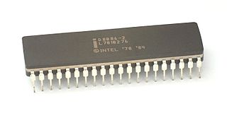
x86 is a family of complex instruction set computer (CISC) instruction set architectures initially developed by Intel based on the Intel 8086 microprocessor and its 8088 variant. The 8086 was introduced in 1978 as a fully 16-bit extension of Intel's 8-bit 8080 microprocessor, with memory segmentation as a solution for addressing more memory than can be covered by a plain 16-bit address. The term "x86" came into being because the names of several successors to Intel's 8086 processor end in "86", including the 80186, 80286, 80386 and 80486 processors. Colloquially, their names were "186", "286", "386" and "486".

<span class="mw-page-title-main">Endianness</span> Order of bytes in a computer word

In computing, endianness is the order or sequence of bytes of a word of digital data in computer memory or data communication which is identified by describing the impact of the "first" bytes, meaning at the smallest address or sent first. Endianness is primarily expressed as big-endian (BE) or little-endian (LE), terms introduced by Danny Cohen into computer science for data ordering in an Internet Experiment Note published in 1980. The adjective endian has its origin in the writings of 18th century Anglo-Irish writer Jonathan Swift. In the 1726 novel Gulliver's Travels, he portrays the conflict between sects of Lilliputians divided into those breaking the shell of a boiled egg from the big end or from the little end.

In computer science, an instruction set architecture (ISA) is an abstract model of a computer. A device that executes instructions described by that ISA, such as a central processing unit (CPU), is called an implementation.
<span class="mw-page-title-main">MCS-51</span> Single chip microcontroller series by Intel

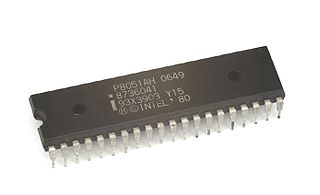
The Intel MCS-51 is a single chip microcontroller (MCU) series developed by Intel in 1980 for use in embedded systems. The architect of the Intel MCS-51 instruction set was John H. Wharton. Intel's original versions were popular in the 1980s and early 1990s, and enhanced binary compatible derivatives remain popular today. It is a complex instruction set computer, but also has some of the features of RISC architectures, such as a large register set and register windows, and has separate memory spaces for program instructions and data.

ARM is a family of RISC instruction set architectures (ISAs) for computer processors. Arm Ltd. develops the ISAs and licenses them to other companies, who build the physical devices that use the instruction set. It also designs and licenses cores that implement these ISAs.

SuperH is a 32-bit reduced instruction set computing (RISC) instruction set architecture (ISA) developed by Hitachi and currently produced by Renesas. It is implemented by microcontrollers and microprocessors for embedded systems.

The DLX is a RISC processor architecture designed by John L. Hennessy and David A. Patterson, the principal designers of the Stanford MIPS and the Berkeley RISC designs (respectively), the two benchmark examples of RISC design.

The x86 instruction set refers to the set of instructions that x86-compatible microprocessors support. The instructions are usually part of an executable program, often stored as a computer file and executed on the processor.

Addressing modes are an aspect of the instruction set architecture in most central processing unit (CPU) designs. The various addressing modes that are defined in a given instruction set architecture define how the machine language instructions in that architecture identify the operand(s) of each instruction. An addressing mode specifies how to calculate the effective memory address of an operand by using information held in registers and/or constants contained within a machine instruction or elsewhere.

In computer engineering, an orthogonal instruction set is an instruction set architecture where all instruction types can use all addressing modes. It is "orthogonal" in the sense that the instruction type and the addressing mode vary independently. An orthogonal instruction set does not impose a limitation that requires a certain instruction to use a specific register so there is little overlapping of instruction functionality.

Berkeley RISC is one of two seminal research projects into reduced instruction set computer (RISC) based microprocessor design taking place under the Defense Advanced Research Projects Agency VLSI Project. RISC was led by David Patterson at the University of California, Berkeley between 1980 and 1984. The other project took place a short distance away at Stanford University under their MIPS effort starting in 1981 and running until 1984.

TLCS is a prefix applied to microcontrollers made by Toshiba. The product line includes multiple families of CISC and RISC architectures. Individual components generally have a part number beginning with "TMP". E.g. the TMP8048AP is a member of the TLCS-48 family.

<span class="mw-page-title-main">History of general-purpose CPUs</span> History of processors used in general purpose computers

The history of general-purpose CPUs is a continuation of the earlier history of computing hardware.

An instruction set architecture (ISA) is an abstract model of a computer, also referred to as computer architecture. A realization of an ISA is called an implementation. An ISA permits multiple implementations that may vary in performance, physical size, and monetary cost ; because the ISA serves as the interface between software and hardware. Software that has been written for an ISA can run on different implementations of the same ISA. This has enabled binary compatibility between different generations of computers to be easily achieved, and the development of computer families. Both of these developments have helped to lower the cost of computers and to increase their applicability. For these reasons, the ISA is one of the most important abstractions in computing today.

eSi-RISC is a configurable CPU architecture. It is available in five implementations: the eSi-1600, eSi-1650, eSi-3200, eSi-3250 and eSi-3264. The eSi-1600 and eSi-1650 feature a 16-bit data-path, while the eSi-32x0s feature 32-bit data-paths, and the eSi-3264 features a mixed 32/64-bit datapath. Each of these processors is licensed as soft IP cores, suitable for integrating into both ASICs and FPGAs.

The EVEX prefix and corresponding coding scheme is an extension to the 32-bit x86 (IA-32) and 64-bit x86-64 (AMD64) instruction set architecture. EVEX is based on, but should not be confused with the MVEX prefix used by the Knights Corner processor.

RISC-V is an open standard instruction set architecture (ISA) based on established reduced instruction set computer (RISC) principles. Unlike most other ISA designs, RISC-V is provided under royalty-free open-source licenses. Many companies are offering or have announced RISC-V hardware; open source operating systems with RISC-V support are available, and the instruction set is supported in several popular software toolchains.

References

Citations

  1. 1 2 3 Verts 2004.
  2. "Understanding ARM Architectures". informIT. 23 August 2010.
  3. Bacon, Jason. "MIPS Instruction Code Formats". Computer Science 315 Lecture Notes. Archived from the original on 2019-07-17. Retrieved 2021-04-09.
  4. Weaver & McKee 2009.
  5. "Effects of 16-bit instructions". Renesas.
  6. SuperH 1996.
  7. SH-5 CPU Core, Volume 1: Architecture (PDF). p. 8.
  8. Lemieux 2004.
  9. "Thumb instruction summary". ARM7TDMI Technical Reference Manual.
  10. MIPS16e2 Application-Specific Extension Technical Reference Manual. MIPS. 26 April 2016.
  11. Power ISA V2.07. IBM.
  12. Alpha Architecture Handbook (PDF). DEC. October 1996. p. 1.4.

Bibliography