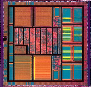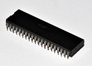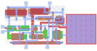
A central processing unit (CPU), also called a central processor, main processor, or just processor, is the most important processor in a given computer. Its electronic circuitry executes instructions of a computer program, such as arithmetic, logic, controlling, and input/output (I/O) operations. This role contrasts with that of external components, such as main memory and I/O circuitry, and specialized coprocessors such as graphics processing units (GPUs).
Processor design is a subfield of computer science and computer engineering (fabrication) that deals with creating a processor, a key component of computer hardware.

The Data Encryption Standard is a symmetric-key algorithm for the encryption of digital data. Although its short key length of 56 bits makes it too insecure for modern applications, it has been highly influential in the advancement of cryptography.

An integrated circuit, also known as a microchip, chip or IC, is a small electronic device made up of multiple interconnected electronic components such as transistors, resistors, and capacitors. These components are etched onto a small piece of semiconductor material, usually silicon. Integrated circuits are used in a wide range of electronic devices, including computers, smartphones, and televisions, to perform various functions such as processing and storing information. They have greatly impacted the field of electronics by enabling device miniaturization and enhanced functionality.

Very-large-scale integration (VLSI) is the process of creating an integrated circuit (IC) by combining millions or billions of MOS transistors onto a single chip. VLSI began in the 1970s when MOS integrated circuit chips were developed and then widely adopted, enabling complex semiconductor and telecommunication technologies. The microprocessor and memory chips are VLSI devices.

The Intel 4004 is a 4-bit central processing unit (CPU) released by Intel Corporation in 1971. Sold for US$60, it was the first commercially produced microprocessor, and the first in a long line of Intel CPUs.

An application-specific integrated circuit is an integrated circuit (IC) chip customized for a particular use, rather than intended for general-purpose use, such as a chip designed to run in a digital voice recorder or a high-efficiency video codec. Application-specific standard product chips are intermediate between ASICs and industry standard integrated circuits like the 7400 series or the 4000 series. ASIC chips are typically fabricated using metal–oxide–semiconductor (MOS) technology, as MOS integrated circuit chips.
Electronic design automation (EDA), also referred to as electronic computer-aided design (ECAD), is a category of software tools for designing electronic systems such as integrated circuits and printed circuit boards. The tools work together in a design flow that chip designers use to design and analyze entire semiconductor chips. Since a modern semiconductor chip can have billions of components, EDA tools are essential for their design; this article in particular describes EDA specifically with respect to integrated circuits (ICs).

The history of computing hardware starting at 1960 is marked by the conversion from vacuum tube to solid-state devices such as transistors and then integrated circuit (IC) chips. Around 1953 to 1959, discrete transistors started being considered sufficiently reliable and economical that they made further vacuum tube computers uncompetitive. Metal–oxide–semiconductor (MOS) large-scale integration (LSI) technology subsequently led to the development of semiconductor memory in the mid-to-late 1960s and then the microprocessor in the early 1970s. This led to primary computer memory moving away from magnetic-core memory devices to solid-state static and dynamic semiconductor memory, which greatly reduced the cost, size, and power consumption of computers. These advances led to the miniaturized personal computer (PC) in the 1970s, starting with home computers and desktop computers, followed by laptops and then mobile computers over the next several decades.

A gate array is an approach to the design and manufacture of application-specific integrated circuits (ASICs) using a prefabricated chip with components that are later interconnected into logic devices according to custom order by adding metal interconnect layers in the factory. It was popular during the upheaval in the semiconductor industry in the 1980s, and its usage declined by the end of the 1990s.
Fabless manufacturing is the design and sale of hardware devices and semiconductor chips while outsourcing their fabrication to a specialized manufacturer called a semiconductor foundry. These foundries are typically, but not exclusively, located in the United States, China, and Taiwan. Fabless companies can benefit from lower capital costs while concentrating their research and development resources on the end market. Some fabless companies and pure play foundries may offer integrated-circuit design services to third parties.

In cryptography, the EFF DES cracker is a machine built by the Electronic Frontier Foundation (EFF) in 1998, to perform a brute force search of the Data Encryption Standard (DES) cipher's key space – that is, to decrypt an encrypted message by trying every possible key. The aim in doing this was to prove that the key size of DES was not sufficient to be secure.

MIFARE is a series of integrated circuit (IC) chips used in contactless smart cards and proximity cards.

Automatic test equipment or automated test equipment (ATE) is any apparatus that performs tests on a device, known as the device under test (DUT), equipment under test (EUT) or unit under test (UUT), using automation to quickly perform measurements and evaluate the test results. An ATE can be a simple computer-controlled digital multimeter, or a complicated system containing dozens of complex test instruments capable of automatically testing and diagnosing faults in sophisticated electronic packaged parts or on wafer testing, including system on chips and integrated circuits.
VLSI Technology, Inc., was an American company that designed and manufactured custom and semi-custom integrated circuits (ICs). The company was based in Silicon Valley, with headquarters at 1109 McKay Drive in San Jose. Along with LSI Logic, VLSI Technology defined the leading edge of the application-specific integrated circuit (ASIC) business, which accelerated the push of powerful embedded systems into affordable products.

Integrated circuit design, semiconductor design, chip design or IC design, is a sub-field of electronics engineering, encompassing the particular logic and circuit design techniques required to design integrated circuits, or ICs. ICs consist of miniaturized electronic components built into an electrical network on a monolithic semiconductor substrate by photolithography.

In integrated circuit design, physical design is a step in the standard design cycle which follows after the circuit design. At this step, circuit representations of the components of the design are converted into geometric representations of shapes which, when manufactured in the corresponding layers of materials, will ensure the required functioning of the components. This geometric representation is called integrated circuit layout. This step is usually split into several sub-steps, which include both design and verification and validation of the layout.
A three-dimensional integrated circuit is a MOS integrated circuit (IC) manufactured by stacking as many as 16 or more ICs and interconnecting them vertically using, for instance, through-silicon vias (TSVs) or Cu-Cu connections, so that they behave as a single device to achieve performance improvements at reduced power and smaller footprint than conventional two dimensional processes. The 3D IC is one of several 3D integration schemes that exploit the z-direction to achieve electrical performance benefits in microelectronics and nanoelectronics.
A Hardware Trojan (HT) is a malicious modification of the circuitry of an integrated circuit. A hardware Trojan is completely characterized by its physical representation and its behavior. The payload of an HT is the entire activity that the Trojan executes when it is triggered. In general, Trojans try to bypass or disable the security fence of a system: for example, leaking confidential information by radio emission. HTs also could disable, damage or destroy the entire chip or components of it.
Hardware obfuscation is a technique by which the description or the structure of electronic hardware is modified to intentionally conceal its functionality, which makes it significantly more difficult to reverse-engineer. In other words, hardware obfuscation modifies the design in such a away that the resulting architecture becomes un-obvious to an adversary. Hardware Obfuscation can be of two types depending on the hardware platform targeted: (a) DSP Core Hardware Obfuscation - this type of obfuscation performs certain high level transformation on the data flow graph representation of DSP core to convert it into an unknown form that reflects an un-obvious architecture at RTL or gate level. This type of obfuscation is also called 'Structural Obfuscation'. Another type of DSP Core Obfuscation method is called 'Functional Obfuscation' - It uses a combination of AES and IP core locking blocks (ILBs) to lock the functionality of the DSP core using key-bits. Without application of correct key sequence, the DSP core produces either wrong output or no output at all (b) Combinational/Sequential Hardware Obfuscation - this type of obfuscation performs changes to the gate level structure of the circuit itself.


