Related Research Articles
A diode is a two-terminal electronic component that conducts current primarily in one direction. It has low resistance in one direction, and high resistance in the other.

The Hall effect is the production of a potential difference across an electrical conductor that is transverse to an electric current in the conductor and to an applied magnetic field perpendicular to the current. It was discovered by Edwin Hall in 1879.
A semiconductor is a material which has an electrical conductivity value falling between that of a conductor, such as copper, and an insulator, such as glass. Its resistivity falls as its temperature rises; metals behave in the opposite way. Its conducting properties may be altered in useful ways by introducing impurities ("doping") into the crystal structure. When two differently doped regions exist in the same crystal, a semiconductor junction is created. The behavior of charge carriers, which include electrons, ions, and electron holes, at these junctions is the basis of diodes, transistors, and most modern electronics. Some examples of semiconductors are silicon, germanium, gallium arsenide, and elements near the so-called "metalloid staircase" on the periodic table. After silicon, gallium arsenide is the second-most common semiconductor and is used in laser diodes, solar cells, microwave-frequency integrated circuits, and others. Silicon is a critical element for fabricating most electronic circuits.

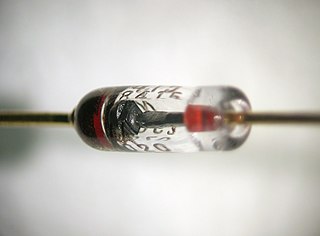
A thermocouple, also known as a "thermoelectrical thermometer", is an electrical device consisting of two dissimilar electrical conductors forming an electrical junction. A thermocouple produces a temperature-dependent voltage as a result of the Seebeck effect, and this voltage can be interpreted to measure temperature. Thermocouples are widely used as temperature sensors.

A thermistor is a semiconductor type of resistor whose resistance is strongly dependent on temperature, more so than in standard resistors. The word thermistor is a portmanteau of thermal and resistor.

Voltage, also known as electric pressure, electric tension, or (electric) potential difference, is the difference in electric potential between two points. In a static electric field, it corresponds to the work needed per unit of charge to move a test charge between the two points. In the International System of Units (SI), the derived unit for voltage is named volt.

A semiconductor device is an electronic component that relies on the electronic properties of a semiconductor material for its function. Its conductivity lies between conductors and insulators. Semiconductor devices have replaced vacuum tubes in most applications. They conduct electric current in the solid state, rather than as free electrons across a vacuum or as free electrons and ions through an ionized gas.

The metal-oxide-semiconductor field-effect transistor is a type of field-effect transistor (FET), most commonly fabricated by the controlled oxidation of silicon. It has an insulated gate, the voltage of which determines the conductivity of the device. This ability to change conductivity with the amount of applied voltage can be used for amplifying or switching electronic signals. A metal-insulator-semiconductor field-effect transistor (MISFET) is a term almost synonymous with MOSFET. Another synonym is IGFET for insulated-gate field-effect transistor.

A bipolar junction transistor (BJT) is a type of transistor that uses both electrons and electron holes as charge carriers. In contrast, a unipolar transistor, such as a field-effect transistor (FET), uses only one kind of charge carrier. A bipolar transistor allows a small current injected at one of its terminals to control a much larger current flowing between the terminals, making the device capable of amplification or switching.
The Fermi level of a solid-state body is the thermodynamic work required to add one electron to the body. It is a thermodynamic quantity usually denoted by µ or EF for brevity. The Fermi level does not include the work required to remove the electron from wherever it came from. A precise understanding of the Fermi level—how it relates to electronic band structure in determining electronic properties; how it relates to the voltage and flow of charge in an electronic circuit—is essential to an understanding of solid-state physics.

The Schottky diode, also known as Schottky barrier diode or hot-carrier diode, is a semiconductor diode formed by the junction of a semiconductor with a metal. It has a low forward voltage drop and a very fast switching action. The cat's-whisker detectors used in the early days of wireless and metal rectifiers used in early power applications can be considered primitive Schottky diodes.
The van der Pauw Method is a technique commonly used to measure the resistivity and the Hall coefficient of a sample. Its power lies in its ability to accurately measure the properties of a sample of any arbitrary shape, as long as the sample is approximately two-dimensional, solid, and the electrodes are placed on its perimeter. The van der Pauw method employs a four-point probe placed around the perimeter of the sample, in contrast to the linear four point probe: this allows the van der Pauw method to provide an average resistivity of the sample, whereas a linear array provides the resistivity in the sensing direction. This difference becomes important for anisotropic materials, which can be properly measured using the Montgomery Method, an extension of the van der Pauw Method.

A p–n junction is a boundary or interface between two types of semiconductor materials, p-type and n-type, inside a single crystal of semiconductor. The "p" (positive) side contains an excess of holes, while the "n" (negative) side contains an excess of electrons in the outer shells of the electrically neutral atoms there. This allows electric current to pass through the junction only in one direction. The p- and n-type regions creating the junction are made by doping the semiconductor, for example by ion implantation, diffusion of dopants, or by epitaxy.
In solid-state physics, the electron mobility characterises how quickly an electron can move through a metal or semiconductor when pulled by an electric field. There is an analogous quantity for holes, called hole mobility. The term carrier mobility refers in general to both electron and hole mobility.
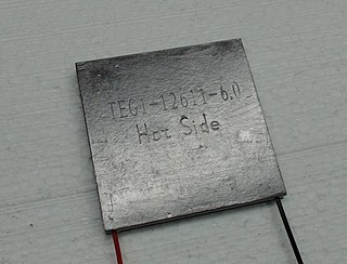
The Seebeck coefficient of a material is a measure of the magnitude of an induced thermoelectric voltage in response to a temperature difference across that material, as induced by the Seebeck effect. The SI unit of the Seebeck coefficient is volts per kelvin (V/K), although it is more often given in microvolts per kelvin (μV/K).
In semiconductor physics, the depletion region, also called depletion layer, depletion zone, junction region, space charge region or space charge layer, is an insulating region within a conductive, doped semiconductor material where the mobile charge carriers have been diffused away, or have been forced away by an electric field. The only elements left in the depletion region are ionized donor or acceptor impurities. This region of uncovered positive and negative ions is called the depletion region due to the depletion of carriers in this region, leaving none to carry a current. Understanding the depletion region is key to explaining modern semiconductor electronics: diodes, bipolar junction transistors, field-effect transistors, and variable capacitance diodes all rely on depletion region phenomena.
p–n junction isolation is a method used to electrically isolate electronic components, such as transistors, on an integrated circuit (IC) by surrounding the components with reverse biased p–n junctions.
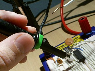
A test probe is a physical device used to connect electronic test equipment to a device under test (DUT). Test probes range from very simple, robust devices to complex probes that are sophisticated, expensive, and fragile. Specific types include test prods, oscilloscope probes and current probes. A test probe is often supplied as a test lead, which includes the probe, cable and terminating connector.
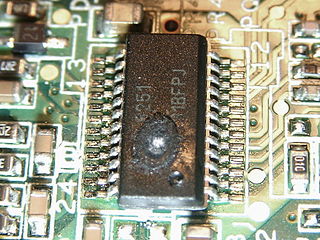
Electronic components have a wide range of failure modes. These can be classified in various ways, such as by time or cause. Failures can be caused by excess temperature, excess current or voltage, ionizing radiation, mechanical shock, stress or impact, and many other causes. In semiconductor devices, problems in the device package may cause failures due to contamination, mechanical stress of the device, or open or short circuits.

The field-effect transistor (FET) is a type of transistor that uses an electric field to control the flow of current in a semiconductor. FETs are devices with three terminals: source, gate, and drain. FETs control the flow of current by the application of a voltage to the gate, which in turn alters the conductivity between the drain and source.
References
- ↑ "The Hot Point Probes". ECE Illinois. Archived from the original on 2010-06-16. Retrieved 2009-10-06.
- ↑ "2.4.7.9 The "hot-probe" experiment". ecee.colorado.edu. Retrieved 27 November 2020.
| | This electronics-related article is a stub. You can help Wikipedia by expanding it. |