Related Research Articles

Solder is a fusible metal alloy used to create a permanent bond between metal workpieces. Solder is melted in order to wet the parts of the joint, where it adheres to and connects the pieces after cooling. Metals or alloys suitable for use as solder should have a lower melting point than the pieces to be joined. The solder should also be resistant to oxidative and corrosive effects that would degrade the joint over time. Solder used in making electrical connections also needs to have favorable electrical characteristics.

Electroplating, also known as electrochemical deposition or electrodeposition, is a process for producing a metal coating on a solid substrate through the reduction of cations of that metal by means of a direct electric current. The part to be coated acts as the cathode of an electrolytic cell; the electrolyte is a solution of a salt of the metal to be coated; and the anode is usually either a block of that metal, or of some inert conductive material. The current is provided by an external power supply.

A printed circuit board (PCB), also called printed wiring board (PWB), is a medium used to connect or "wire" components to one another in a circuit. It takes the form of a laminated sandwich structure of conductive and insulating layers: each of the conductive layers is designed with a pattern of traces, planes and other features etched from one or more sheet layers of copper laminated onto and/or between sheet layers of a non-conductive substrate. Electrical components may be fixed to conductive pads on the outer layers in the shape designed to accept the component's terminals, generally by means of soldering, to both electrically connect and mechanically fasten them to it. Another manufacturing process adds vias, plated-through holes that allow interconnections between layers.

Surface-mount technology (SMT), originally called planar mounting, is a method in which the electrical components are mounted directly onto the surface of a printed circuit board (PCB). An electrical component mounted in this manner is referred to as a surface-mount device (SMD). In industry, this approach has largely replaced the through-hole technology construction method of fitting components, in large part because SMT allows for increased manufacturing automation which reduces cost and improves quality. It also allows for more components to fit on a given area of substrate. Both technologies can be used on the same board, with the through-hole technology often used for components not suitable for surface mounting such as large transformers and heat-sinked power semiconductors.

Chrome plating is a technique of electroplating a thin layer of chromium onto a metal object. A chrome plated part is called chrome, or is said to have been chromed. The chromium layer can be decorative, provide corrosion resistance, facilitate cleaning, and increase surface hardness. Sometimes, a less expensive substitute for chrome such as nickel may be used for aesthetic purposes.

Wave soldering is a bulk soldering process used for the manufacturing of printed circuit boards. The circuit board is passed over a pan of molten solder in which a pump produces an upwelling of solder that looks like a standing wave. As the circuit board makes contact with this wave, the components become soldered to the board. Wave soldering is used for both through-hole printed circuit assemblies, and surface mount. In the latter case, the components are glued onto the surface of a printed circuit board (PCB) by placement equipment, before being run through the molten solder wave. Wave soldering is mainly used in soldering of through hole components.
Plating is a finishing process in which a metal is deposited on a surface. Plating has been done for hundreds of years; it is also critical for modern technology. Plating is used to decorate objects, for corrosion inhibition, to improve solderability, to harden, to improve wearability, to reduce friction, to improve paint adhesion, to alter conductivity, to improve IR reflectivity, for radiation shielding, and for other purposes. Jewelry typically uses plating to give a silver or gold finish.

Gold plating is a method of depositing a thin layer of gold onto the surface of another metal, most often copper or silver, by chemical or electrochemical plating. Plating refers to modern coating methods, such as the ones used in the electronics industry, whereas gilding is the decorative covering of an object with gold, which typically involve more traditional methods and much larger objects.
A via is an electrical connection between two or more metal layers, and are commonly used in printed circuit boards (PCB). Essentially a via is a small drilled hole that goes through two or more adjacent layers; the hole is plated with metal that forms an electrical connection through the insulating layers.

Electroless nickel-phosphorus plating, also referred to as E-nickel, is a chemical process that deposits an even layer of nickel-phosphorus alloy on the surface of a solid substrate, like metal or plastic. The process involves dipping the substrate in a water solution containing nickel salt and a phosphorus-containing reducing agent, usually a hypophosphite salt. It is the most common version of electroless nickel plating and is often referred by that name. A similar process uses a borohydride reducing agent, yielding a nickel-boron coating instead.

Flat no-leads packages such as quad-flat no-leads (QFN) and dual-flat no-leads (DFN) physically and electrically connect integrated circuits to printed circuit boards. Flat no-leads, also known as micro leadframe (MLF) and SON, is a surface-mount technology, one of several package technologies that connect ICs to the surfaces of PCBs without through-holes. Flat no-lead is a near chip scale plastic encapsulated package made with a planar copper lead frame substrate. Perimeter lands on the package bottom provide electrical connections to the PCB. Flat no-lead packages usually, but not always, include an exposed thermally conductive pad to improve heat transfer out of the IC. Heat transfer can be further facilitated by metal vias in the thermal pad. The QFN package is similar to the quad-flat package (QFP), and a ball grid array (BGA).
HASL or HAL is a type of finish used on printed circuit boards (PCBs).
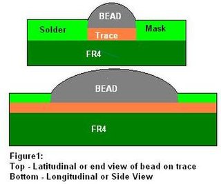
Bead probe technology (BPT) is technique used to provide electrical access to printed circuit board (PCB) circuitry for performing in-circuit testing (ICT). It makes use of small beads of solder placed onto the board's traces to allow measuring and controlling of the signals using a test probe. This permits test access to boards on which standard ICT test pads are not feasible due to space constraints.
Black oxide or blackening is a conversion coating for ferrous materials, stainless steel, copper and copper based alloys, zinc, powdered metals, and silver solder. It is used to add mild corrosion resistance, for appearance, and to minimize light reflection. To achieve maximal corrosion resistance the black oxide must be impregnated with oil or wax. One of its advantages over other coatings is its minimal buildup.
Electroless nickel immersion gold (ENIG or ENi/IAu), also known as immersion gold (Au), chemical Ni/Au or soft gold, is a metal plating process used in the manufacture of printed circuit boards (PCBs), to avoid oxidation and improve the solderability of copper contacts and plated through-holes. It consists of an electroless nickel plating, covered with a thin layer of gold, which protects the nickel from oxidation. The gold is typically applied by quick immersion in a solution containing gold salts. Some of the nickel is oxidized to Ni2+ while the gold is reduced to metallic state. A variant of this process adds a thin layer of electroless palladium over the nickel, a process known by the acronym ENEPIG.
Organic solderability preservative or OSP is a method for coating of printed circuit boards. It uses a water-based organic compound that selectively bonds to copper and protects the copper until soldering.

Soldering is a process of joining two metal surfaces together using a filler metal called solder. The soldering process involves heating the surfaces to be joined and melting the solder, which is then allowed to cool and solidify, creating a strong and durable joint.
Ellington Electronics Technology Group 依頓電子科技股份有限公司 is one of the leading printed circuit board (PCB) manufacturers in China. It is a Hong Kong based company which is listed on the Shanghai Stock Exchange on 1 July 2014. In Year 2018, the company was ranked Top 10 in China and 41st in the world by revenue.
Pad cratering is a mechanically induced fracture in the resin between copper foil and outermost layer of fiberglass of a printed circuit board (PCB). It may be within the resin or at the resin to fiberglass interface.
Flowers of sulfur (FOS) testing was developed to determine the porosity of metallic coatings susceptible to sulfur induced corrosion [see below ASTM B809-95(2018)]. Applicable substrates are silver, copper, copper alloys and any other metal or metal alloy with which sulfur will react. For porosity testing, coatings can be single or multiple layers of any metal that is not corroded and sealed by a self-limiting reaction in the reducing sulfur environment of the FOS test. The simplest recommended technique is to identify any porosity of the coating as revealed by the presence of surface spots. These surface spots form where the environmental sulfur has penetrated and reacted with the base metal, producing a metal sulfide. Chalcocite, copper (I) sulfide is dark-grey to black. Silver (I) sulfide is also grey-black.
References
- ↑ Slocum, Dan Jr. (2003-09-25). "Surface Finishes Utilized in the PCB Industry" (PDF). Archived from the original (PDF) on 2013-11-05. Retrieved 2018-11-15.