Related Research Articles

A transistor is a semiconductor device used to amplify or switch electrical signals and power. It is one of the basic building blocks of modern electronics. It is composed of semiconductor material, usually with at least three terminals for connection to an electronic circuit. A voltage or current applied to one pair of the transistor's terminals controls the current through another pair of terminals. Because the controlled (output) power can be higher than the controlling (input) power, a transistor can amplify a signal. Some transistors are packaged individually, but many more in miniature form are found embedded in integrated circuits. Because transistors are the key active components in practically all modern electronics, many people consider them one of the 20th century's greatest inventions.

A semiconductor device is an electronic component that relies on the electronic properties of a semiconductor material for its function. Its conductivity lies between conductors and insulators. Semiconductor devices have replaced vacuum tubes in most applications. They conduct electric current in the solid state, rather than as free electrons across a vacuum or as free electrons and ions through an ionized gas.

The metal–oxide–semiconductor field-effect transistor is a type of field-effect transistor (FET), most commonly fabricated by the controlled oxidation of silicon. It has an insulated gate, the voltage of which determines the conductivity of the device. This ability to change conductivity with the amount of applied voltage can be used for amplifying or switching electronic signals. The term metal–insulator–semiconductor field-effect transistor (MISFET) is almost synonymous with MOSFET. Another near-synonym is insulated-gate field-effect transistor (IGFET).

The junction-gate field-effect transistor (JFET) is one of the simplest types of field-effect transistor. JFETs are three-terminal semiconductor devices that can be used as electronically controlled switches or resistors, or to build amplifiers.

A high-electron-mobility transistor, also known as heterostructure FET (HFET) or modulation-doped FET (MODFET), is a field-effect transistor incorporating a junction between two materials with different band gaps as the channel instead of a doped region. A commonly used material combination is GaAs with AlGaAs, though there is wide variation, dependent on the application of the device. Devices incorporating more indium generally show better high-frequency performance, while in recent years, gallium nitride HEMTs have attracted attention due to their high-power performance. Like other FETs, HEMTs are used in integrated circuits as digital on-off switches. FETs can also be used as amplifiers for large amounts of current using a small voltage as a control signal. Both of these uses are made possible by the FET’s unique current–voltage characteristics. HEMT transistors are able to operate at higher frequencies than ordinary transistors, up to millimeter wave frequencies, and are used in high-frequency products such as cell phones, satellite television receivers, voltage converters, and radar equipment. They are widely used in satellite receivers, in low power amplifiers and in the defense industry.
The threshold voltage, commonly abbreviated as Vth or VGS(th), of a field-effect transistor (FET) is the minimum gate-to-source voltage (VGS) that is needed to create a conducting path between the source and drain terminals. It is an important scaling factor to maintain power efficiency.

A fin field-effect transistor (FinFET) is a multigate device, a MOSFET built on a substrate where the gate is placed on two, three, or four sides of the channel or wrapped around the channel, forming a double or even multi gate structure. These devices have been given the generic name "FinFETs" because the source/drain region forms fins on the silicon surface. The FinFET devices have significantly faster switching times and higher current density than planar CMOS technology.

An organic field-effect transistor (OFET) is a field-effect transistor using an organic semiconductor in its channel. OFETs can be prepared either by vacuum evaporation of small molecules, by solution-casting of polymers or small molecules, or by mechanical transfer of a peeled single-crystalline organic layer onto a substrate. These devices have been developed to realize low-cost, large-area electronic products and biodegradable electronics. OFETs have been fabricated with various device geometries. The most commonly used device geometry is bottom gate with top drain and source electrodes, because this geometry is similar to the thin-film silicon transistor (TFT) using thermally grown SiO2 as gate dielectric. Organic polymers, such as poly(methyl-methacrylate) (PMMA), can also be used as dielectric. One of the benefits of OFETs, especially compared with inorganic TFTs, is their unprecedented physical flexibility, which leads to biocompatible applications, for instance in the future health care industry of personalized biomedicines and bioelectronics.

A VMOS transistor is a type of metal–oxide–semiconductor field-effect transistor (MOSFET). VMOS is also used to describe the V-groove shape vertically cut into the substrate material.
Capacitance–voltage profiling is a technique for characterizing semiconductor materials and devices. The applied voltage is varied, and the capacitance is measured and plotted as a function of voltage. The technique uses a metal–semiconductor junction or a p–n junction or a MOSFET to create a depletion region, a region which is empty of conducting electrons and holes, but may contain ionized donors and electrically active defects or traps. The depletion region with its ionized charges inside behaves like a capacitor. By varying the voltage applied to the junction it is possible to vary the depletion width. The dependence of the depletion width upon the applied voltage provides information on the semiconductor's internal characteristics, such as its doping profile and electrically active defect densities., Measurements may be done at DC, or using both DC and a small-signal AC signal, or using a large-signal transient voltage.

A multigate device, multi-gate MOSFET or multi-gate field-effect transistor (MuGFET) refers to a metal–oxide–semiconductor field-effect transistor (MOSFET) that has more than one gate on a single transistor. The multiple gates may be controlled by a single gate electrode, wherein the multiple gate surfaces act electrically as a single gate, or by independent gate electrodes. A multigate device employing independent gate electrodes is sometimes called a multiple-independent-gate field-effect transistor (MIGFET). The most widely used multi-gate devices are the FinFET and the GAAFET, which are non-planar transistors, or 3D transistors.
Nanocircuits are electrical circuits operating on the nanometer scale. This is well into the quantum realm, where quantum mechanical effects become very important. One nanometer is equal to 10−9 meters or a row of 10 hydrogen atoms. With such progressively smaller circuits, more can be fitted on a computer chip. This allows faster and more complex functions using less power. Nanocircuits are composed of three different fundamental components. These are transistors, interconnections, and architecture, all fabricated on the nanometer scale.
A transistor is a semiconductor device with at least three terminals for connection to an electric circuit. In the common case, the third terminal controls the flow of current between the other two terminals. This can be used for amplification, as in the case of a radio receiver, or for rapid switching, as in the case of digital circuits. The transistor replaced the vacuum-tube triode, also called a (thermionic) valve, which was much larger in size and used significantly more power to operate. The first transistor was successfully demonstrated on December 23, 1947, at Bell Laboratories in Murray Hill, New Jersey. Bell Labs was the research arm of American Telephone and Telegraph (AT&T). The three individuals credited with the invention of the transistor were William Shockley, John Bardeen and Walter Brattain. The introduction of the transistor is often considered one of the most important inventions in history.
The gate oxide is the dielectric layer that separates the gate terminal of a MOSFET from the underlying source and drain terminals as well as the conductive channel that connects source and drain when the transistor is turned on. Gate oxide is formed by thermal oxidation of the silicon of the channel to form a thin insulating layer of silicon dioxide. The insulating silicon dioxide layer is formed through a process of self-limiting oxidation, which is described by the Deal–Grove model. A conductive gate material is subsequently deposited over the gate oxide to form the transistor. The gate oxide serves as the dielectric layer so that the gate can sustain as high as 1 to 5 MV/cm transverse electric field in order to strongly modulate the conductance of the channel.
For electronic semiconductor devices, a native transistor is a variety of the MOS field-effect transistor that is intermediate between enhancement and depletion modes. Most common is the n-channel native transistor.

In field-effect transistors (FETs), depletion mode and enhancement mode are two major transistor types, corresponding to whether the transistor is in an on state or an off state at zero gate–source voltage.
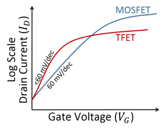
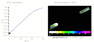
The tunnel field-effect transistor (TFET) is an experimental type of transistor. Even though its structure is very similar to a metal–oxide–semiconductor field-effect transistor (MOSFET), the fundamental switching mechanism differs, making this device a promising candidate for low power electronics. TFETs switch by modulating quantum tunneling through a barrier instead of modulating thermionic emission over a barrier as in traditional MOSFETs. Because of this, TFETs are not limited by the thermal Maxwell–Boltzmann tail of carriers, which limits MOSFET drain current subthreshold swing to about 60 mV/decade of current at room temperature.

The field-effect transistor (FET) is a type of transistor that uses an electric field to control the flow of current in a semiconductor. It comes in two types: junction-gate FET (JFET) and metal-oxide-semiconductor FET (MOSFET). FETs have three terminals: source, gate, and drain. FETs control the flow of current by the application of a voltage to the gate, which in turn alters the conductivity between the drain and source.
A quantum field-effect transistor (QFET) or quantum-well field-effect transistor (QWFET) is a type of MOSFET that takes advantage of quantum tunneling to greatly increase the speed of transistor operation by eliminating the traditional transistor's area of electron conduction which typically causes carriers to slow down by a factor of 3000. The result is an increase in logic speed by a factor of 10 with a simultaneous reduction in component power requirement and size also by a factor of 10. It achieves these things through a manufacturing process known as rapid thermal processing (RTP) that uses ultrafine layers of construction materials.

A field-effect transistor-based biosensor, also known as a biosensor field-effect transistor, field-effect biosensor (FEB), or biosensor MOSFET, is a field-effect transistor that is gated by changes in the surface potential induced by the binding of molecules. When charged molecules, such as biomolecules, bind to the FET gate, which is usually a dielectric material, they can change the charge distribution of the underlying semiconductor material resulting in a change in conductance of the FET channel. A Bio-FET consists of two main compartments: one is the biological recognition element and the other is the field-effect transistor. The BioFET structure is largely based on the ion-sensitive field-effect transistor (ISFET), a type of metal–oxide–semiconductor field-effect transistor (MOSFET) where the metal gate is replaced by an ion-sensitive membrane, electrolyte solution, and reference electrode.
References
- ↑ Kranti, A.; Yan, R.; Lee, C. -W.; Ferain, I.; Yu, R.; Dehdashti Akhavan, N.; Razavi, P.; Colinge, J. P. (2010). "Junctionless nanowire transistor (JNT): Properties and design guidelines". 2010 Proceedings of the European Solid State Device Research Conference. p. 357. doi:10.1109/ESSDERC.2010.5618216. ISBN 978-1-4244-6658-0.
- ↑ Larrieu, Guilhem; Han, X.-L. (2013). "Vertical nanowire array-based field effect transistors for ultimate scaling". Nanoscale. 5 (6): 2437–2441. Bibcode:2013Nanos...5.2437L. doi:10.1039/c3nr33738c. eISSN 2040-3372. ISSN 2040-3364. PMID 23403487.
- ↑ Colinge, J. P.; Kranti, A.; Yan, R.; Lee, C. W.; Ferain, I.; Yu, R.; Dehdashti Akhavan, N.; Razavi, P. (2011). "Junctionless Nanowire Transistor (JNT): Properties and design guidelines". Solid-State Electronics. 65–66: 33–37. Bibcode:2011SSEle..65...33C. doi:10.1016/j.sse.2011.06.004. S2CID 8382657.
- ↑ Yu, Ran (2013). "Junctionless nanowire transistor fabricated with high mobility Ge channel". Physica Status Solidi RRL. 8: 65–68. doi:10.1002/pssr.201300119. S2CID 93197577.
Junctionless Nanowire Transistor: Properties and Device Guidelines
Ferain Junctionless Transistors (pdf)
| | This electronics-related article is a stub. You can help Wikipedia by expanding it. |