Kendall Square Research

Last updated
KSR1 logo KSR1-logo-small.jpg
KSR1 logo

Kendall Square Research (KSR) was a supercomputer company headquartered originally in Kendall Square in Cambridge, Massachusetts in 1986, near Massachusetts Institute of Technology (MIT). It was co-founded by Steven Frank [1] and Henry Burkhardt III, who had formerly helped found Data General and Encore Computer and was one of the original team that designed the PDP-8. KSR produced two models of supercomputer, the KSR1 and KSR2. It went bankrupt in 1994.

Contents

Technology

The KSR systems ran a specially customized version of the OSF/1 operating system, a Unix variant, with programs compiled by a KSR-specific port of the Green Hills Software C and FORTRAN compilers. The architecture was shared memory implemented as a cache-only memory architecture or "COMA". Being all cache, memory dynamically migrated and replicated in a coherent manner based on the access pattern of individual processors. The processors were arranged in a hierarchy of rings, and the operating system mediated process migration and device access. Instruction decode was hardwired, and pipelining was used. Each KSR1 processor was a custom 64-bit reduced instruction set computing (RISC) CPU clocked at 20 MHz and capable of a peak output of 20 million instructions per second (MIPS) and 40 million floating-point operations per second (MFLOPS). Up to 1088 of these processors could be arranged in a single system, with a minimum of eight. The KSR2 doubled the clock rate to 40 MHz and supported over 5000 processors. The KSR-1 chipset was fabricated by Sharp Corporation while the KSR-2 chipset was built by Hewlett-Packard.

Software

Besides the traditional scientific applications, KSR with Oracle Corporation, addressed the massively parallel database market for commercial applications. The KSR-1 and -2 supported Micro Focus COBOL and C/C++ programming languages, and the Oracle database and the MATISSE OODBMS from ADB, Inc. Their own product, the KSR Query Decomposer, complemented the functions of the Oracle product for SQL uses. The TUXEDO transaction monitor for OLTP was also provided. The KAP program (Kuck & Associate Preprocessor) provided for pre-processing for source code analysis and parallelization. The runtime environment was termed PRESTO, and was a POSIX compliant multithreading manager.

KSR2 ALLCACHE Processor, Router and Directory (APRD) board with two APRD cells Ksr cell top.jpg
KSR2 ALLCACHE Processor, Router and Directory (APRD) board with two APRD cells

Hardware

The KSR-1 processor was implemented as a four-chip set in 1.2 micrometer complementary metal–oxide–semiconductor (CMOS). These chips were: the cell execution unit, the floating point unit, the arithmetic logic unit, and the external I/O unit (XIO). The CEU handled instruction fetch (two per clock), and all operations involving memory, such as loads and stores. 40-bit addresses were used, going to full 64-bit addresses later. The integer unit had 32, 64-bit-wide registers. The floating point unit is discussed below. The XIO had the capacity of 30 MB/s throughput to I/O devices. It included 64 control and data registers.

The KSR processor was a 2-wide VLIW, with instructions of 6 types: memory reference (load and store), execute, control flow, memory control, I/O, and inserted. Execute instructions included arithmetic, logical, and type conversion. They were usually triadic register in format. Control flow refers to branches and jumps. Branch instructions were two cycles. The programmer (or compiler) could implicitly control the quashing behavior of the subsequent two instructions that would be initiated during the branch. The choices were: always retain the results, retain results if branch test is true, or retain results if branch test is false. Memory control provided synchronization primitives. I/O instructions were provided. Inserted instructions were forced into a flow by a coprocessor. Inserted load and store were used for direct memory access (DMA) transfers. Inserted memory instructions were used to maintain cache coherency. New coprocessors could be interfaced with the inserted instruction mechanism. IEEE standard floating point arithmetic was supported. Sixty-four 64-bit wide registers were included.

The following example of KSR assembly performs an indirect procedure call to an address held in the procedure's constant block, saving the return address in register c14. It also saves the frame pointer, loads integer register zero with the value 3, and increments integer register 31 without changing the condition codes. Most instructions have a delay slot of 2 cycles and the delay slots are not interlocked, so must be scheduled explicitly, else the resulting hazard means wrong values are sometimes loaded.

finop   ; movb8_8 %i2,%c10 finop   ; cxnop finop   ; cxnop add8.ntr 75,%i31,%i31 ; ld8 8(%c10),%c4 finop   ; st8 %fp,504(%sp) finop                   ; cxnop movi8 3, %i0            ; jsr %c14,16(%c4) 

In the KSR design, all of the memory was treated as cache. The design called for no home location- to reduce storage overheads and to software transparently, dynamically migrate/replicate memory based on where it was utilized; a Harvard architecture, separate bus for instructions and memory was used. Each node board contained 256 KB of I-cache and D-cache, essentially primary cache. At each node was 32 MB of memory for main cache. The system level architecture was shared virtual memory, which was physically distributed in the machine. The programmer or application only saw one contiguous address space, which was spanned by a 40-bit address. Traffic between nodes traveled at up to 4 gigabytes per second. The 32 megabytes per node, in aggregate, formed the physical memory of the machine.

Specialized input/output processors could be used in the system, providing scalable I/O. A 1088 node KSR1 could have 510 I/O channels with an aggregate in excess of 15 GB/s. Interfaces such as Ethernet, FDDI, and HIPPI were supported.

History

As the company scaled up quickly to enter production, they moved in the late 1980s to 170 Tracer Lane, Waltham, Massachusetts.

KSR refocused its efforts from the scientific to the commercial marketplace, with emphasis on parallel relational databases and OLTP operations. It then got out of the hardware business, but continued to market some of its data warehousing and analysis software products.

The first KSR1 system was installed in 1991. With new processor hardware, new memory hardware and a novel memory architecture, a new compiler port, a new port of a relatively new operating system, and exposed memory hazards, early systems were noted for frequent system crashes. KSR called their cache-only memory architecture (COMA) by the trade name Allcache; reliability problems with early systems earned it the nickname Allcrash, although memory was not necessarily the root cause of crashes. A few KSR1 models were sold, and as the KSR2 was being rolled out, the company collapsed amid accounting irregularities involving the overstatement of revenue.

KSR used a proprietary processor because 64-bit processors were not commercially available. However, this put the small company in the difficult position of doing both processor design and system design. The KSR processors were introduced in 1991 at 20 MHz and 40 MFlops. At that time, the 32-bit Intel 80486 ran at 50 MHz and 50 MFlops. When the 64-bit DEC Alpha was introduced in 1992, it ran at up to 192 MHz and 192 MFlops, while the 1992 KSR2 ran at 40 MHz and 80 MFlops.

One customer of the KSR2, the Pacific Northwest National Laboratory, a United States Department of Energy facility, purchased an enormous number of spare parts, and kept their machines running for years after the demise of KSR.

KSR, along with many of its competitors (see below), went bankrupt during the collapse of the supercomputer market in the early 1990s. KSR went out of business in February 1994, when their stock was delisted from the stock exchange.

Competition

KSR's competitors included MasPar Computer Corporation, Thinking Machines, Meiko Scientific, and various old-line (and still surviving) companies like IBM and Intel.

Related Research Articles

MIPS is a family of reduced instruction set computer (RISC) instruction set architectures (ISA) developed by MIPS Computer Systems, now MIPS Technologies, based in the United States.

<span class="mw-page-title-main">SPARC</span> RISC instruction set architecture

SPARC is a reduced instruction set computer (RISC) instruction set architecture originally developed by Sun Microsystems. Its design was strongly influenced by the experimental Berkeley RISC system developed in the early 1980s. First developed in 1986 and released in 1987, SPARC was one of the most successful early commercial RISC systems, and its success led to the introduction of similar RISC designs from many vendors through the 1980s and 1990s.

The Intel i860 is a RISC microprocessor design introduced by Intel in 1989. It is one of Intel's first attempts at an entirely new, high-end instruction set architecture since the failed Intel iAPX 432 from the beginning of the 1980s. It was the world's first million-transistor chip. It was released with considerable fanfare, slightly obscuring the earlier Intel i960, which was successful in some niches of embedded systems. The i860 never achieved commercial success and the project was terminated in the mid-1990s.

<span class="mw-page-title-main">Digital signal processor</span> Specialized microprocessor optimized for digital signal processing

A digital signal processor (DSP) is a specialized microprocessor chip, with its architecture optimized for the operational needs of digital signal processing. DSPs are fabricated on metal–oxide–semiconductor (MOS) integrated circuit chips. They are widely used in audio signal processing, telecommunications, digital image processing, radar, sonar and speech recognition systems, and in common consumer electronic devices such as mobile phones, disk drives and high-definition television (HDTV) products.

<span class="mw-page-title-main">CDC Cyber</span> Range of mainframe-class supercomputers

The CDC Cyber range of mainframe-class supercomputers were the primary products of Control Data Corporation (CDC) during the 1970s and 1980s. In their day, they were the computer architecture of choice for scientific and mathematically intensive computing. They were used for modeling fluid flow, material science stress analysis, electrochemical machining analysis, probabilistic analysis, energy and academic computing, radiation shielding modeling, and other applications. The lineup also included the Cyber 18 and Cyber 1000 minicomputers. Like their predecessor, the CDC 6600, they were unusual in using the ones' complement binary representation.

<span class="mw-page-title-main">CDC STAR-100</span>

The CDC STAR-100 is a vector supercomputer that was designed, manufactured, and marketed by Control Data Corporation (CDC). It was one of the first machines to use a vector processor to improve performance on appropriate scientific applications. It was also the first supercomputer to use integrated circuits and the first to be equipped with one million words of computer memory.

<span class="mw-page-title-main">Emotion Engine</span> Central processing unit by Sony Computer Entertainment and Toshiba

The Emotion Engine is a central processing unit developed and manufactured by Sony Computer Entertainment and Toshiba for use in the PlayStation 2 video game console. It was also used in early PlayStation 3 models sold in Japan and North America to provide PlayStation 2 game support. Mass production of the Emotion Engine began in 1999 and ended in late 2012 with the discontinuation of the PlayStation 2.

The POWER1 is a multi-chip CPU developed and fabricated by IBM that implemented the POWER instruction set architecture (ISA). It was originally known as the RISC System/6000 CPU or, when in an abbreviated form, the RS/6000 CPU, before introduction of successors required the original name to be replaced with one that used the same naming scheme (POWERn) as its successors in order to differentiate it from the newer designs.

In computing, a word is the natural unit of data used by a particular processor design. A word is a fixed-sized datum handled as a unit by the instruction set or the hardware of the processor. The number of bits or digits in a word is an important characteristic of any specific processor design or computer architecture.

<span class="mw-page-title-main">R10000</span> MIPS microprocessor

The R10000, code-named "T5", is a RISC microprocessor implementation of the MIPS IV instruction set architecture (ISA) developed by MIPS Technologies, Inc. (MTI), then a division of Silicon Graphics, Inc. (SGI). The chief designers are Chris Rowen and Kenneth C. Yeager. The R10000 microarchitecture is known as ANDES, an abbreviation for Architecture with Non-sequential Dynamic Execution Scheduling. The R10000 largely replaces the R8000 in the high-end and the R4400 elsewhere. MTI was a fabless semiconductor company; the R10000 was fabricated by NEC and Toshiba. Previous fabricators of MIPS microprocessors such as Integrated Device Technology (IDT) and three others did not fabricate the R10000 as it was more expensive to do so than the R4000 and R4400.

<span class="mw-page-title-main">R4000</span> MIPS microprocessor

The R4000 is a microprocessor developed by MIPS Computer Systems that implements the MIPS III instruction set architecture (ISA). Officially announced on 1 October 1991, it was one of the first 64-bit microprocessors and the first MIPS III implementation. In the early 1990s, when RISC microprocessors were expected to replace CISC microprocessors such as the Intel i486, the R4000 was selected to be the microprocessor of the Advanced Computing Environment (ACE), an industry standard that intended to define a common RISC platform. ACE ultimately failed for a number of reasons, but the R4000 found success in the workstation and server markets.

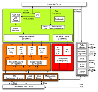
The R8000 is a microprocessor chipset developed by MIPS Technologies, Inc. (MTI), Toshiba, and Weitek. It was the first implementation of the MIPS IV instruction set architecture. The R8000 is also known as the TFP, for Tremendous Floating-Point, its name during development.

<span class="mw-page-title-main">CDC 6000 series</span>

The CDC 6000 series is a discontinued family of mainframe computers manufactured by Control Data Corporation in the 1960s. It consisted of the CDC 6200, CDC 6300, CDC 6400, CDC 6500, CDC 6600 and CDC 6700 computers, which were all extremely rapid and efficient for their time. Each is a large, solid-state, general-purpose, digital computer that performs scientific and business data processing as well as multiprogramming, multiprocessing, Remote Job Entry, time-sharing, and data management tasks under the control of the operating system called SCOPE. By 1970 there also was a time-sharing oriented operating system named KRONOS. They were part of the first generation of supercomputers. The 6600 was the flagship of Control Data's 6000 series.

<span class="mw-page-title-main">SGI Origin 2000</span> Series of server computers

The SGI Origin 2000 is a family of mid-range and high-end server computers developed and manufactured by Silicon Graphics (SGI). They were introduced in 1996 to succeed the SGI Challenge and POWER Challenge. At the time of introduction, these ran the IRIX operating system, originally version 6.4 and later, 6.5. A variant of the Origin 2000 with graphics capability is known as the Onyx2. An entry-level variant based on the same architecture but with a different hardware implementation is known as the Origin 200. The Origin 2000 was succeeded by the Origin 3000 in July 2000, and was discontinued on June 30, 2002.

<span class="mw-page-title-main">Alpha 21264</span> RISC microprocessor

The Alpha 21264 is a Digital Equipment Corporation RISC microprocessor launched on 19 October 1998. The 21264 implemented the Alpha instruction set architecture (ISA).

The SPARC64 V (Zeus) is a SPARC V9 microprocessor designed by Fujitsu. The SPARC64 V was the basis for a series of successive processors designed for servers, and later, supercomputers.

The HITAC S-810 is a family of vector supercomputers developed, manufactured and marketed by Hitachi. The S-810, first announced in August 1982, was the second Japanese supercomputer, following the Fujitsu VP-200 but predating the NEC SX-2. The S-810 was Hitachi's first supercomputer, although the company had previously built a vector processor, the IAP.

Zero ASIC Corporation, formerly Adapteva, Inc., is a fabless semiconductor company focusing on low power many core microprocessor design. The company was the second company to announce a design with 1,000 specialized processing cores on a single integrated circuit.

Sunway, or Shenwei,, is a series of computer microprocessors, developed by Jiangnan Computing Lab (江南计算技术研究所) in Wuxi, China. It uses a reduced instruction set computer (RISC) architecture, but details are still sparse.

IBM POWER is a reduced instruction set computer (RISC) instruction set architecture (ISA) developed by IBM. The name is an acronym for Performance Optimization With Enhanced RISC.

References

  1. "Virtual Shared Memory Symposium" . Retrieved 2009-01-23.

Further reading