The theorem results in maximum power transfer from the power source to the load, and not maximum efficiency of useful power out of total power consumed. If the load resistance is made larger than the source resistance, then efficiency increases (since a higher percentage of the source power is transferred to the load), but the magnitude of the load power decreases (since the total circuit resistance increases).[2] If the load resistance is made smaller than the source resistance, then efficiency decreases (since most of the power ends up being dissipated in the source). Although the total power dissipated increases (due to a lower total resistance), the amount dissipated in the load decreases.
The theorem states how to choose (so as to maximize power transfer) the load resistance, once the source resistance is given. It is a common misconception to apply the theorem in the opposite scenario. It does not say how to choose the source resistance for a given load resistance. In fact, the source resistance that maximizes power transfer from a voltage source is always zero (the hypothetical ideal voltage source), regardless of the value of the load resistance.
The mathematics of the theorem also applies to other physical interactions, such as:[2][3]
mechanical collisions between two objects,
the sharing of charge between two capacitors,
liquid flow between two cylinders,
the transmission and reflection of light at the boundary between two media.
Maximizing power transfer versus power efficiency
Simplified model for powering a load with resistance RL by a source with voltage VS and resistance RS.
The theorem was originally misunderstood (notably by Joule[4]) to imply that a system consisting of an electric motor driven by a battery could not be more than 50% efficient, since the power dissipated as heat in the battery would always be equal to the power delivered to the motor when the impedances were matched.
In 1880 this assumption was shown to be false by either Edison or his colleague Francis Robbins Upton, who realized that maximum efficiency was not the same as maximum power transfer.
To achieve maximum efficiency, the resistance of the source (whether a battery or a dynamo) could be (or should be) made as close to zero as possible. Using this new understanding, they obtained an efficiency of about 90%, and proved that the electric motor was a practical alternative to the heat engine.
The red curve shows the power in the load, normalized relative to its maximum possible. The dark blue curve shows the efficiency η.
The efficiency η is the ratio of the power dissipated by the load resistance RL to the total power dissipated by the circuit (which includes the voltage source's resistance of RS as well as RL):
Consider three particular cases (note that voltage sources must have some resistance):
If , then Efficiency approaches 0% if the load resistance approaches zero (a short circuit), since all power is consumed in the source and no power is consumed in the short.
If , then Efficiency is only 50% if the load resistance equals the source resistance (which is the condition of maximum power transfer).
If , then Efficiency approaches 100% if the load resistance approaches infinity (though the total power level tends towards zero) or if the source resistance approaches zero. Using a large ratio is called impedance bridging.
Calculus-based proof for purely resistive circuits
In the simplified model of powering a load with resistance RL by a source with voltage VS and source resistanceRS, then by Ohm's law the resulting current I is simply the source voltage divided by the total circuit resistance:
The power PL dissipated in the load is the square of the current multiplied by the resistance:
The value of RL for which this expression is a maximum could be calculated by differentiating it, but it is easier to calculate the value of RL for which the denominator:
is a minimum. The result will be the same in either case. Differentiating the denominator with respect to RL:
For a maximum or minimum, the first derivative is zero, so
or
In practical resistive circuits, RS and RL are both positive, so the positive sign in the above is the correct solution.
To find out whether this solution is a minimum or a maximum, the denominator expression is differentiated again:
This is always positive for positive values of and , showing that the denominator is a minimum, and the power is therefore a maximum, when:
The above proof assumes fixed source resistance . When the source resistance can be varied, power transferred to the load can be increased by reducing . For example, a 100 Volt source with an of will deliver 250 watts of power to a load; reducing to increases the power delivered to 1000 watts.
Note that this shows that maximum power transfer can also be interpreted as the load voltage being equal to one-half of the Thevenin voltage equivalent of the source.[5]
In reactive circuits
The power transfer theorem also applies when the source and/or load are not purely resistive.
A refinement of the maximum power theorem says that any reactive components of source and load should be of equal magnitude but opposite sign. (See below for a derivation.)
This means that the source and load impedances should be complex conjugates of each other.
In the case of purely resistive circuits, the two concepts are identical.
Physically realizable sources and loads are not usually purely resistive, having some inductive or capacitive components, and so practical applications of this theorem, under the name of complex conjugate impedance matching, do, in fact, exist.
If the source is totally inductive (capacitive), then a totally capacitive (inductive) load, in the absence of resistive losses, would receive 100% of the energy from the source but send it back after a quarter cycle.
The resultant circuit is nothing other than a resonant LC circuit in which the energy continues to oscillate to and fro. This oscillation is called reactive power.
Power factor correction (where an inductive reactance is used to "balance out" a capacitive one), is essentially the same idea as complex conjugate impedance matching although it is done for entirely different reasons.
For a fixed reactive source, the maximum power theorem maximizes the real power (P) delivered to the load by complex conjugate matching the load to the source.
For a fixed reactive load, power factor correction minimizes the apparent power (S) (and unnecessary current) conducted by the transmission lines, while maintaining the same amount of real power transfer.
This is done by adding a reactance to the load to balance out the load's own reactance, changing the reactive load impedance into a resistive load impedance.
Proof
source and load impedance diagram
In this diagram, AC power is being transferred from the source, with phasor magnitude of voltage (positive peak voltage) and fixed source impedance (S for source), to a load with impedance (L for load), resulting in a (positive) magnitude of the current phasor . This magnitude results from dividing the magnitude of the source voltage by the magnitude of the total circuit impedance:
The average power dissipated in the load is the square of the current multiplied by the resistive portion (the real part) of the load impedance :
where and denote the resistances, that is the real parts, and and denote the reactances, that is the imaginary parts, of respectively the source and load impedances and .
To determine, for a given source voltage and impedance the value of the load impedance for which this expression for the power yields a maximum, one first finds, for each fixed positive value of , the value of the reactive term for which the denominator:
is a minimum. Since reactances can be negative, this is achieved by adapting the load reactance to:
This reduces the above equation to:
and it remains to find the value of which maximizes this expression. This problem has the same form as in the purely resistive case, and the maximizing condition therefore is
The two maximizing conditions:
describe the complex conjugate of the source impedance, denoted by and thus can be concisely combined to:
1 2 Harrison, Mark (2013-02-22). "Physical collisions and the maximum power theorem: an analogy between mechanical and electrical situations". Physics Education. 48 (2): 207–211. doi:10.1088/0031-9120/48/2/207. ISSN0031-9120. S2CID120330420.
The characteristic impedance or surge impedance (usually written Z0) of a uniform transmission line is the ratio of the amplitudes of voltage and current of a single wave propagating along the line; that is, a wave travelling in one direction in the absence of reflections in the other direction. Alternatively, and equivalently, it can be defined as the input impedance of a transmission line when its length is infinite. Characteristic impedance is determined by the geometry and materials of the transmission line and, for a uniform line, is not dependent on its length. The SI unit of characteristic impedance is the ohm.
In electrical engineering, impedance is the opposition to alternating current presented by the combined effect of resistance and reactance in a circuit.
The electrical resistance of an object is a measure of its opposition to the flow of electric current. Its reciprocal quantity is electrical conductance, measuring the ease with which an electric current passes. Electrical resistance shares some conceptual parallels with mechanical friction. The SI unit of electrical resistance is the ohm, while electrical conductance is measured in siemens (S).
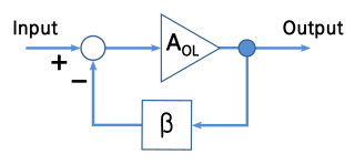
A negative-feedback amplifier is an electronic amplifier that subtracts a fraction of its output from its input, so that negative feedback opposes the original signal. The applied negative feedback can improve its performance and reduces sensitivity to parameter variations due to manufacturing or environment. Because of these advantages, many amplifiers and control systems use negative feedback.
In electronics, negative resistance (NR) is a property of some electrical circuits and devices in which an increase in voltage across the device's terminals results in a decrease in electric current through it.
In electronics, impedance matching is the practice of designing or adjusting the input impedance or output impedance of an electrical device for a desired value. Often, the desired value is selected to maximize power transfer or minimize signal reflection. For example, impedance matching typically is used to improve power transfer from a radio transmitter via the interconnecting transmission line to the antenna. Signals on a transmission line will be transmitted without reflections if the transmission line is terminated with a matching impedance.
In electronics, a voltage divider (also known as a potential divider) is a passive linear circuit that produces an output voltage (Vout) that is a fraction of its input voltage (Vin). Voltage division is the result of distributing the input voltage among the components of the divider. A simple example of a voltage divider is two resistors connected in series, with the input voltage applied across the resistor pair and the output voltage emerging from the connection between them.
An LC circuit, also called a resonant circuit, tank circuit, or tuned circuit, is an electric circuit consisting of an inductor, represented by the letter L, and a capacitor, represented by the letter C, connected together. The circuit can act as an electrical resonator, an electrical analogue of a tuning fork, storing energy oscillating at the circuit's resonant frequency.
In audio engineering and sound recording, a high impedance bridging, voltage bridging, or simply bridging connection is one in which the load impedance is much larger than the source impedance. The load measures the source's voltage while minimally drawing current or affecting it.
The input impedance of an electrical network is the measure of the opposition to current (impedance), both static (resistance) and dynamic (reactance), into a load network that is external to the electrical source network. The input admittance is a measure of the load network's propensity to draw current. The source network is the portion of the network that transmits power, and the load network is the portion of the network that consumes power.
The output impedance of an electrical network is the measure of the opposition to current flow (impedance), both static (resistance) and dynamic (reactance), into the load network being connected that is internal to the electrical source. The output impedance is a measure of the source's propensity to drop in voltage when the load draws current, the source network being the portion of the network that transmits and the load network being the portion of the network that consumes.
In electrical engineering and electronics, a network is a collection of interconnected components. Network analysis is the process of finding the voltages across, and the currents through, all network components. There are many techniques for calculating these values; however, for the most part, the techniques assume linear components. Except where stated, the methods described in this article are applicable only to linear network analysis.
In an electric circuit, instantaneous power is the time rate of flow of energy past a given point of the circuit. In alternating current circuits, energy storage elements such as inductors and capacitors may result in periodic reversals of the direction of energy flow. Its SI unit is the watt.
In electronics, a current divider is a simple linear circuit that produces an output current (IX) that is a fraction of its input current (IT). Current division refers to the splitting of current between the branches of the divider. The currents in the various branches of such a circuit will always divide in such a way as to minimize the total energy expended.
Ripple in electronics is the residual periodic variation of the DC voltage within a power supply which has been derived from an alternating current (AC) source. This ripple is due to incomplete suppression of the alternating waveform after rectification. Ripple voltage originates as the output of a rectifier or from generation and commutation of DC power.
An attenuator is an electronic device that reduces the power of a signal without appreciably distorting its waveform.
An L pad is a network composed of two impedances that typically resemble the letter capital "L" when drawn on a schematic circuit diagram. It is commonly used for attenuation and for impedance matching.
In electrical engineering, the power gain of an electrical network is the ratio of an output power to an input power. Unlike other signal gains, such as voltage and current gain, "power gain" may be ambiguous as the meaning of terms "input power" and "output power" is not always clear. Three important power gains are operating power gain, transducer power gain and available power gain. Note that all these definitions of power gains employ the use of average power quantities and therefore the term "average" is often suppressed, which can be confusing at occasions.
The gyrator–capacitor model - sometimes also the capacitor-permeance model - is a lumped-element model for magnetic circuits, that can be used in place of the more common resistance–reluctance model. The model makes permeance elements analogous to electrical capacitance rather than electrical resistance. Windings are represented as gyrators, interfacing between the electrical circuit and the magnetic model.
An RLC circuit is an electrical circuit consisting of a resistor (R), an inductor (L), and a capacitor (C), connected in series or in parallel. The name of the circuit is derived from the letters that are used to denote the constituent components of this circuit, where the sequence of the components may vary from RLC.
References
H.W. Jackson (1959) Introduction to Electronic Circuits, Prentice-Hall.
This page is based on this Wikipedia article Text is available under the CC BY-SA 4.0 license; additional terms may apply. Images, videos and audio are available under their respective licenses.