Related Research Articles

Nanocrystalline silicon (nc-Si), sometimes also known as microcrystalline silicon (μc-Si), is a form of porous silicon. It is an allotropic form of silicon with paracrystalline structure—is similar to amorphous silicon (a-Si), in that it has an amorphous phase. Where they differ, however, is that nc-Si has small grains of crystalline silicon within the amorphous phase. This is in contrast to polycrystalline silicon (poly-Si) which consists solely of crystalline silicon grains, separated by grain boundaries. The difference comes solely from the grain size of the crystalline grains. Most materials with grains in the micrometre range are actually fine-grained polysilicon, so nanocrystalline silicon is a better term. The term Nanocrystalline silicon refers to a range of materials around the transition region from amorphous to microcrystalline phase in the silicon thin film. The crystalline volume fraction is another criterion to describe the materials in this transition zone.

A solar cell, or photovoltaic cell, is an electrical device that converts the energy of light directly into electricity by the photovoltaic effect, which is a physical and chemical phenomenon. It is a form of photoelectric cell, defined as a device whose electrical characteristics, such as current, voltage, or resistance, vary when exposed to light. Individual solar cell devices are often the electrical building blocks of photovoltaic modules, known colloquially as solar panels. The common single junction silicon solar cell can produce a maximum open-circuit voltage of approximately 0.5 to 0.6 volts.

A protocrystalline phase is a distinct phase occurring during crystal growth which evolves into a microcrystalline form. The term is typically associated with silicon films in optical applications such as solar cells.
Third-generation photovoltaic cells are solar cells that are potentially able to overcome the Shockley–Queisser limit of 31–41% power efficiency for single bandgap solar cells. This includes a range of alternatives to cells made of semiconducting p-n junctions and thin film cells. Common third-generation systems include multi-layer ("tandem") cells made of amorphous silicon or gallium arsenide, while more theoretical developments include frequency conversion,, hot-carrier effects and other multiple-carrier ejection techniques.
The Staebler–Wronski Effect (SWE) refers to light-induced metastable changes in the properties of hydrogenated amorphous silicon.
Bosch Solar Energy AG was a German solar wafer and solar cell manufacturer, based in Erfurt, which specialized in crystalline silicon-based photovoltaic (PV) products, as well as thin-film modules using amorphous silicon and CIGS absorber materials. The company consisted of the various divisions for silicon, wafers, solar cells and modules, research and production facilities in Germany and France and plans were made to open a production line in Malaysia. It has been listed on the German stock exchange since 30 September 2005 and on 19 December 2005 its shares were admitted to the TecDAX. The enterprise was founded in 1997 as ErSol Solarstrom GmbH & Co. KG.

Multi-junction (MJ) solar cells are solar cells with multiple p–n junctions made of different semiconductor materials. Each material's p-n junction will produce electric current in response to different wavelengths of light. The use of multiple semiconducting materials allows the absorbance of a broader range of wavelengths, improving the cell's sunlight to electrical energy conversion efficiency.
Monocrystalline silicon, more often called single-crystal silicon, in short mono c-Si or mono-Si, is the base material for silicon-based discrete components and integrated circuits used in virtually all modern electronic equipment. Mono-Si also serves as a photovoltaic, light-absorbing material in the manufacture of solar cells.
TEL Solar, formerly Oerlikon Solar, is a manufacturer of production equipment for the manufacturing of thin-film silicon cells, headquartered in Trübbach, Switzerland, near the border to Liechtenstein. The Japanese electronics and semiconductor company Tokyo Electron acquired the company of about 650 employees from OC Oerlikon in November 2012.

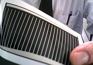
A thin-film solar cell is a second generation solar cell that is made by depositing one or more thin layers, or thin film (TF) of photovoltaic material on a substrate, such as glass, plastic or metal. Thin-film solar cells are commercially used in several technologies, including cadmium telluride (CdTe), copper indium gallium diselenide (CIGS), and amorphous thin-film silicon.
A copper indium gallium selenide solar cell is a thin-film solar cell used to convert sunlight into electric power. It is manufactured by depositing a thin layer of copper, indium, gallium and selenium on glass or plastic backing, along with electrodes on the front and back to collect current. Because the material has a high absorption coefficient and strongly absorbs sunlight, a much thinner film is required than of other semiconductor materials.
A plasmonic-enhanced solar cell, commonly referred to simply as plasmonic solar cell, is a type of solar cell that converts light into electricity with the assistance of plasmons, but where the photovoltaic effect occurs in another material.

Crystalline silicon (c-Si) is the crystalline forms of silicon, either polycrystalline silicon, or monocrystalline silicon. Crystalline silicon is the dominant semiconducting material used in photovoltaic technology for the production of solar cells. These cells are assembled into solar panels as part of a photovoltaic system to generate solar power from sunlight.
Christopher R. Wronski was an electrical engineer and Professor Emeritus at Pennsylvania State University, noted for his pioneering research in photovoltaic cells including discovery of amorphous silicon solar cell and the Staebler–Wronski effect.
There are currently many research groups active in the field of photovoltaics in universities and research institutions around the world. This research can be categorized into three areas: making current technology solar cells cheaper and/or more efficient to effectively compete with other energy sources; developing new technologies based on new solar cell architectural designs; and developing new materials to serve as more efficient energy converters from light energy into electric current or light absorbers and charge carriers.

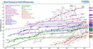
Solar cell efficiency refers to the portion of energy in the form of sunlight that can be converted via photovoltaics into electricity by the solar cell.

Polycrystalline silicon, or multicrystalline silicon, also called polysilicon, poly-Si, or mc-Si, is a high purity, polycrystalline form of silicon, used as a raw material by the solar photovoltaic and electronics industry.
David L. Staebler is an American electrical engineer.

Amorphous silicon (a-Si) is the non-crystalline form of silicon used for solar cells and thin-film transistors in LCDs.

Subhendu Guha is an Indian American photovoltaic scientist who invented flexible Solar shingles. He is known for his pioneering work in Amorphous silicon and Nanocrystalline silicon. In 1998 Dr Guha invented flexible solar cells that can be directly applied to residential roof tops.
References
- ↑ J. Meier, S. Dubail, D. Fischer, J. A. Anna Selvan, N. Pellaton Vaucher, R. Platz, C. Hof, R. Flückiger, U. Kroll, N. Wyrsch, P. Torres, H. Keppner, A. Shah, K.-D. Ufert, "The 'Micromorph' Solar Cells: a New Way to High Efficiency Thin Film Silicon Solar Cells", Proceedings of the 13th EC Photovoltaic Solar Energy Conference, Nice, October 1995, pp. 1445–1450.
- ↑ O. Papathanasiou, "A good day for Ms. Schönefeld-Schnuck PI 5/2009 page 44", http://www.op-solar.de/pdfs/A%20good%20day%20for%20Schoenefeld-Schnuck.pdf