Nanoelectromechanical relay

Last updated

A nanoelectromechanical (NEM) relay is an electrically actuated switch that is built on the nanometer scale using semiconductor fabrication techniques. They are designed to operate in replacement of, or in conjunction with, traditional semiconductor logic. While the mechanical nature of NEM relays makes them switch much slower than solid-state relays, they have many advantageous properties, such as zero current leakage and low power consumption, which make them potentially useful in next generation computing.

Contents

A typical NEM Relay requires a potential on the order of the tens of volts in order to "pull in" and have contact resistances on the order of gigaohms. Coating contact surfaces with platinum can reduce achievable contact resistance to as low as 3 kΩ. [1] Compared to transistors, NEM relays switch relatively slowly, on the order of nanoseconds. [2]

Operation

Schematic of a three terminal electromechanical relay Schematic of a three terminal electromechanical relay.jpg
Schematic of a three terminal electromechanical relay

A NEM relay can be fabricated in two, three, or four terminal configurations. A three terminal relay is composed of a source (input), drain (output), and a gate (actuation terminal). Attached to the source is a cantilevered beam that can be bent into contact with the drain in order to make an electrical connection. When a significant voltage differential is applied between the beam and gate, and the electrostatic force overcomes the elastic force of the beam enough to bend it into contact with the drain, the device "pulls in" and forms an electrical connection. In the off position, the source and drain are separated by an air gap. This physical separation allows NEM relays to have zero current leakage, and very sharp on/off transitions. [3]

The nonlinear nature of the electric field, and adhesion between the beam and drain cause the device to "pull out" and lose connection at a lower voltage than the voltage at which it pulls in. This hysteresis effect means there is a voltage between the pull in voltage, and the pull out voltage that will not change the state of the relay, no matter what its initial state is. This property is very useful in applications where information needs to be stored in the circuit, such as in static random-access memory. [1]

Fabrication

NEM relays are usually fabricated using surface micromachining techniques typical of microelectromechanical systems (MEMS). [4] Laterally actuated relays are constructed by first depositing two or more layers of material on a silicon wafer. The upper structural layer is photolithographically patterned in order to form isolated blocks of the uppermost material. The layer below is then selectively etched away, leaving thin structures, such as the relay's beam, cantilevered above the wafer, and free to bend laterally. [1] A common set of materials used in this process is polysilicon as the upper structural layer, and silicon dioxide as the sacrificial lower layer.

NEM relays can be fabricated using a back end of line compatible process, allowing them to be built on top of CMOS. [1] This property allows NEM relays to be used to significantly reduce the area of certain circuits. For example, a CMOS-NEM relay hybrid inverter occupies 0.03 μm2, one-third the area of a 45 nm CMOS inverter. [5]

History

The first switch made using silicon micro-machining techniques was fabricated in 1978. [6] Those switches were made using bulk micromachining processes and electroplating. [7] In the 1980s, surface micromachining techniques were developed [8] and the technology was applied to the fabrication of switches, allowing for smaller, more efficient relays. [9]

A major early application of MEMS relays was for switching radio frequency signals at which solid-state relays had poor performance. [10] The switching time for these early relays was above 1 μs. By shrinking dimensions below one micrometer, [11] and moving into the nano scale, MEMS switches have achieved switching times in the ranges of hundreds of nanoseconds. [5]

Applications

Mechanical computing

Due to transistor leakage, there is a limit to the theoretical efficiency of CMOS logic. This efficiency barrier ultimately prevents continued increases in computing power in power-constrained applications. [12] While NEM relays have significant switching delays, their small size and fast switching speed when compared to other relays means that mechanical computing utilizing NEM Relays could prove a viable replacement for typical CMOS based integrated circuits, and break this CMOS efficiency barrier. [3] [2]

A NEM relay switches mechanically about 1000 times slower than a solid-state transistor takes to switch electrically. While this makes using NEM relays for computing a significant challenge, their low resistance would allow many NEM relays to be chained together and switch all at once, performing a single large calculation. [2] On the other hand, transistor logic has to be implemented in small cycles of calculations, because their high resistance does not allow many transistors to be chained together while maintaining signal integrity. Therefore, it would be possible to create a mechanical computer using NEM relays that operates at a much lower clock speed than CMOS logic, but performs larger, more complex calculations during each cycle. This would allow a NEM relay based logic to perform to standards comparable to current CMOS logic. [2]

There are many applications, such as in the automotive, aerospace, or geothermal exploration businesses, in which it would be beneficial to have a microcontroller that could operate at very high temperatures. However, at high temperatures, semiconductors used in typical microcontrollers begin to fail as the electrical properties of the materials they are made of degrade, and the transistors no longer function. NEM relays do not rely on the electrical properties of materials to actuate, so a mechanical computer utilizing NEM relays would be able to operate in such conditions. NEM relays have been successfully tested at up to 500 °C, but could theoretically withstand much higher temperatures. [13]

Field-programmable gate arrays

The zero leakage current, low energy usage, and ability to be layered on top of CMOS properties of NEM relays make them a promising candidate for usage as routing switches in field-programmable gate arrays (FPGA). A FPGA utilizing a NEM relay to replace each routing switch and its corresponding static random-access memory block could allow for a significant reduction in programming delay, power leakage, and chip area compared to a typical 22nm CMOS based FPGA. [14] This area reduction mainly comes from the fact that the NEM relay routing layer can be built on top of the CMOS layer of the FPGA.

See also

Related Research Articles

<span class="mw-page-title-main">Logic gate</span> Device performing a Boolean function

A logic gate is a device that performs a Boolean function, a logical operation performed on one or more binary inputs that produces a single binary output. Depending on the context, the term may refer to an ideal logic gate, one that has, for instance, zero rise time and unlimited fan-out, or it may refer to a non-ideal physical device.

<span class="mw-page-title-main">MEMS</span> Very small devices that incorporate moving components

MEMS is the technology of microscopic devices incorporating both electronic and moving parts. MEMS are made up of components between 1 and 100 micrometres in size, and MEMS devices generally range in size from 20 micrometres to a millimetre, although components arranged in arrays can be more than 1000 mm2. They usually consist of a central unit that processes data and several components that interact with the surroundings.

<span class="mw-page-title-main">Transistor</span> Solid-state electrically operated switch also used as an amplifier

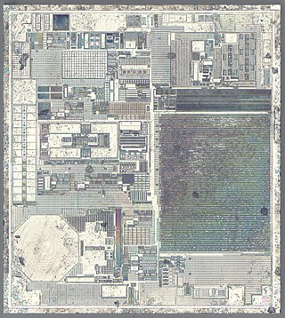
A transistor is a semiconductor device used to amplify or switch electrical signals and power. It is one of the basic building blocks of modern electronics. It is composed of semiconductor material, usually with at least three terminals for connection to an electronic circuit. A voltage or current applied to one pair of the transistor's terminals controls the current through another pair of terminals. Because the controlled (output) power can be higher than the controlling (input) power, a transistor can amplify a signal. Some transistors are packaged individually, but many more in miniature form are found embedded in integrated circuits. Because transistors are the key active components in practically all modern electronics, many people consider them one of the 20th century's greatest inventions.

<span class="mw-page-title-main">CMOS</span> Technology for constructing integrated circuits

Complementary metal–oxide–semiconductor is a type of metal–oxide–semiconductor field-effect transistor (MOSFET) fabrication process that uses complementary and symmetrical pairs of p-type and n-type MOSFETs for logic functions. CMOS technology is used for constructing integrated circuit (IC) chips, including microprocessors, microcontrollers, memory chips, and other digital logic circuits. CMOS technology is also used for analog circuits such as image sensors, data converters, RF circuits, and highly integrated transceivers for many types of communication.

<span class="mw-page-title-main">Nanoelectromechanical systems</span> Class of devices for nanoscale functionality

Nanoelectromechanical systems (NEMS) are a class of devices integrating electrical and mechanical functionality on the nanoscale. NEMS form the next logical miniaturization step from so-called microelectromechanical systems, or MEMS devices. NEMS typically integrate transistor-like nanoelectronics with mechanical actuators, pumps, or motors, and may thereby form physical, biological, and chemical sensors. The name derives from typical device dimensions in the nanometer range, leading to low mass, high mechanical resonance frequencies, potentially large quantum mechanical effects such as zero point motion, and a high surface-to-volume ratio useful for surface-based sensing mechanisms. Applications include accelerometers and sensors to detect chemical substances in the air.

Surface micromachining builds microstructures by deposition and etching structural layers over a substrate. This is different from Bulk micromachining, in which a silicon substrate wafer is selectively etched to produce structures.

<span class="mw-page-title-main">Fin field-effect transistor</span> Type of non-planar transistor

A fin field-effect transistor (FinFET) is a multigate device, a MOSFET built on a substrate where the gate is placed on two, three, or four sides of the channel or wrapped around the channel, forming a double or even multi gate structure. These devices have been given the generic name "FinFETs" because the source/drain region forms fins on the silicon surface. The FinFET devices have significantly faster switching times and higher current density than planar CMOS technology.

<span class="mw-page-title-main">Comb drive</span>

Comb-drives are microelectromechanical actuators, often used as linear actuators, which utilize electrostatic forces that act between two electrically conductive combs. Comb drive actuators typically operate at the micro- or nanometer scale and are generally manufactured by bulk micromachining or surface micromachining a silicon wafer substrate.

SONOS, short for "silicon–oxide–nitride–oxide–silicon", more precisely, "polycrystalline silicon"—"silicon dioxide"—"silicon nitride"—"silicon dioxide"—"silicon", is a cross sectional structure of MOSFET (metal–oxide–semiconductor field-effect transistor), realized by P.C.Y. Chen of Fairchild Camera and Instrument in 1977. This structure is often used for non-volatile memories, such as EEPROM and flash memories. It is sometimes used for TFT LCD displays. It is one of CTF (charge trap flash) variants. It is distinguished from traditional non-volatile memory structures by the use of silicon nitride (Si3N4 or Si9N10) instead of "polysilicon-based FG (floating-gate)" for the charge storage material. A further variant is "SHINOS" ("silicon"—"hi-k"—"nitride"—"oxide"—"silicon"), which is substituted top oxide layer with high-κ material. Another advanced variant is "MONOS" ("metal–oxide–nitride–oxide–silicon"). Companies offering SONOS-based products include Cypress Semiconductor, Macronix, Toshiba, United Microelectronics Corporation and Floadia.

<span class="mw-page-title-main">Multigate device</span> MOS field-effect transistor with more than one gate

A multigate device, multi-gate MOSFET or multi-gate field-effect transistor (MuGFET) refers to a metal–oxide–semiconductor field-effect transistor (MOSFET) that has more than one gate on a single transistor. The multiple gates may be controlled by a single gate electrode, wherein the multiple gate surfaces act electrically as a single gate, or by independent gate electrodes. A multigate device employing independent gate electrodes is sometimes called a multiple-independent-gate field-effect transistor (MIGFET). The most widely used multi-gate devices are the FinFET and the GAAFET, which are non-planar transistors, or 3D transistors.

Microoptoelectromechanical systems (MOEMS), also known as optical MEMS, are integrations of mechanical, optical, and electrical systems that involve sensing or manipulating optical signals at a very small size. MOEMS includes a wide variety of devices, for example optical switch, optical cross-connect, tunable VCSEL, microbolometers. These devices are usually fabricated using micro-optics and standard micromachining technologies using materials like silicon, silicon dioxide, silicon nitride and gallium arsenide.

<span class="mw-page-title-main">Electromechanics</span> Multidisciplinary field of engineering

In engineering, electromechanics combines processes and procedures drawn from electrical engineering and mechanical engineering. Electromechanics focuses on the interaction of electrical and mechanical systems as a whole and how the two systems interact with each other. This process is especially prominent in systems such as those of DC or AC rotating electrical machines which can be designed and operated to generate power from a mechanical process (generator) or used to power a mechanical effect (motor). Electrical engineering in this context also encompasses electronics engineering.

Microelectromechanical system oscillators are devices that generate highly stable reference frequencies used to sequence electronic systems, manage data transfer, define radio frequencies, and measure elapsed time. The core technologies used in MEMS oscillators have been in development since the mid-1960s, but have only been sufficiently advanced for commercial applications since 2006. MEMS oscillators incorporate MEMS resonators, which are microelectromechanical structures that define stable frequencies. MEMS clock generators are MEMS timing devices with multiple outputs for systems that need more than a single reference frequency. MEMS oscillators are a valid alternative to older, more established quartz crystal oscillators, offering better resilience against vibration and mechanical shock, and reliability with respect to temperature variation.

<span class="mw-page-title-main">Tunnel field-effect transistor</span>

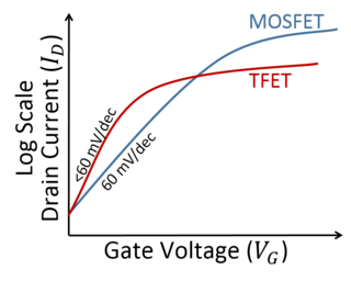
The tunnel field-effect transistor (TFET) is an experimental type of transistor. Even though its structure is very similar to a metal–oxide–semiconductor field-effect transistor (MOSFET), the fundamental switching mechanism differs, making this device a promising candidate for low power electronics. TFETs switch by modulating quantum tunneling through a barrier instead of modulating thermionic emission over a barrier as in traditional MOSFETs. Because of this, TFETs are not limited by the thermal Maxwell–Boltzmann tail of carriers, which limits MOSFET drain current subthreshold swing to about 60 mV/decade of current at room temperature.

<span class="mw-page-title-main">Roger T. Howe</span>

Roger Thomas Howe is the William E. Ayer Professor of Electrical Engineering at Stanford University. He earned a B.S. degree in physics from Harvey Mudd College and M.S. and Ph.D. degrees in electrical engineering from the University of California, Berkeley in 1981 and 1984, respectively. He was a faculty member at Carnegie-Mellon University from 1984-1985, at the Massachusetts Institute of Technology from 1985-1987, and at UC Berkeley between 1987-2005, where he was the Robert S. Pepper Distinguished Professor. He has been a faculty member of the School of Engineering at Stanford since 2005.

Bijan Davari is an Iranian-American electrical engineer. He is an IBM Fellow and Vice President at IBM Thomas J Watson Research Center, Yorktown Hts, NY. His pioneering work in the miniaturization of semiconductor devices changed the world of computing. His research led to the first generation of voltage-scaled deep-submicron CMOS with sufficient performance to totally replace bipolar technology in IBM mainframes and enable new high-performance UNIX servers. As head of IBM’s Semiconductor Research Center (SRDC), he led IBM into the use of Copper interconnect, silicon on insulator (SOI), and Embedded DRAM before its rivals. He is a member of the U.S. National Academy of Engineering and is known for his seminal contributions to the field of CMOS technology. He is an IEEE Fellow, recipient of the J J Ebers Award in 2005 and IEEE Andrew S. Grove Award in 2010. At the present time, he leads the Next Generation Systems Area of research.

A piezoelectric microelectromechanical system (piezoMEMS) is a miniature or microscopic device that uses piezoelectricity to generate motion and carry out its tasks. It is a microelectromechanical system that takes advantage of an electrical potential that appears under mechanical stress. PiezoMEMS can be found in a variety of applications, such as switches, inkjet printer heads, sensors, micropumps, and energy harvesters.

<span class="mw-page-title-main">T-MOS thermal sensor</span>

TMOS is a type of thermal sensor consisting in a micromachined thermally isolated transistor fabricated using CMOS-SOI(Silicon on Insulator) MEMS(Micro electro-mechanical system) technology. It has been developed in the last decade by the Technion - Israel Institute of Technology. A thermal sensor is a device able to detect the thermal radiation emitted by an object located in the FOV(Field Of View) of the sensor. Infrared radiation striking the sensor produces a change in the temperature of the device that as a consequence generates an electric output signal proportional to the incident IR power. The sensor is able to measure the temperature of the object radiating thanks to the information contained in the impinging radiation, exploiting in this sense Stefan - Boltzmann law. TMOS detector has two important characteristics that make it different from others: it's an active and uncooled sensor.

References

  1. 1 2 3 4 Parsa, Roozbeh; Lee, W. Scott; Shavezipur, Mohammad; Provine, J; Mitra, Subhashish; Wong, H.-S. Philip; Howe, Roger T. (7 March 2013). "Laterally Actuated Platinum-Coated Polysilicon NEM Relays". Journal of Microelectromechanical Systems. 22 (3): 768–778. doi:10.1109/JMEMS.2013.2244779. S2CID   24310991.
  2. 1 2 3 4 Chen, Fred; Kam, Hei; Markovic, Dejan; Liu, Tsu-Jae King; Stojanovic, Vladimir; Alon, Elad (2008-11-10). "Integrated Circuit Design with NEM Relays". ICCAD '08 Proceedings of the 2008 IEEE/ACM International Conference on Computer-Aided Design. pp. 750–757. ISBN   9781424428205 . Retrieved 29 October 2014.
  3. 1 2 Chen, F; Spencer, M; Nathanael, R; ChengCheng, Wang; Fariborzi, H; Gupta, A; Hei, Kam; Pott, V; Kaeseok, Jeon; Tsu-Jae, King Liu; Markovic, D.; Stojanovic, V.; Alon, E. (February 2010). "Demonstration of integrated micro-electro-mechanical switch circuits for VLSI applications". 2010 IEEE International Solid-State Circuits Conference - (ISSCC). pp. 150–151. CiteSeerX   10.1.1.460.2411 . doi:10.1109/ISSCC.2010.5434010. ISBN   978-1-4244-6033-5. S2CID   8905826.
  4. Kam, Hei; Pott, V; Nathanael, R; Jeon, Jaeseok; Alon, E; Liu, Tsu-Jae King (December 2009). "Design and reliability of a micro-relay technology for zero-standby-power digital logic applications". 2009 IEEE International Electron Devices Meeting (IEDM). pp. 1–4. doi:10.1109/IEDM.2009.5424218. ISBN   978-1-4244-5639-0. S2CID   41011570.
  5. 1 2 Akarvardar, K; Elata, D; Parsa, R; Wan, G. C.; Yoo, K; Provine, J; Peumans, P; Howe, R.T.; Wong, H.-S.P. (10 December 2007). "Design Considerations for Complementary Nanoelectromechanical Logic Gates". 2007 IEEE International Electron Devices Meeting. pp. 299–302. doi:10.1109/IEDM.2007.4418930. ISBN   978-1-4244-1507-6. S2CID   41342836.
  6. Petersen, Kurt (October 1978). "Dynamic Micromechanics on Silicon: Techniques and Devices". IEEE Transactions on Electron Devices. 25 (10): 1241–1250. Bibcode:1978ITED...25.1241P. doi:10.1109/T-ED.1978.19259. S2CID   31025130.
  7. Petersen, Kurt (May 1982). "Silicon as a mechanical material". Proceedings of the IEEE. 70 (5): 420–457. Bibcode:1982IEEEP..70..420P. doi:10.1109/PROC.1982.12331. S2CID   15378788.
  8. Bustillo, J.M.; Howe, R.T.; Muller, R.S. (August 1998). "Surface micromachining for microelectromechanical systems". Proceedings of the IEEE. 86 (8): 1552–1574. CiteSeerX   10.1.1.120.4059 . doi:10.1109/5.704260.
  9. Sakata, M (February 1989). "An electrostatic microactuator for electro-mechanical relay". An Investigation of Micro Structures, Sensors, Actuators, Machines and Robots. IEEE Micro Electro Mechanical Systems, Proceedings. pp. 149–151. doi:10.1109/MEMSYS.1989.77980. S2CID   111117216.
  10. Yao, J.J.; Chang, M.F. (June 1995). "A Surface Micromachined Miniature Switch for Telecommunications Applications with Signal Frequencies from DC up to 4 GHZ". Proceedings of the International Solid-State Sensors and Actuators Conference - TRANSDUCERS '95. Vol. 2. pp. 384–387. doi:10.1109/SENSOR.1995.721827. S2CID   110197804.
  11. Jang, Weon Wi; Lee, Jeong Oen; Yoon, Jun-Bo; Kim, Min-Sang; Lee, Ji-Myoung; Kim, Sung-Min; Cho, Keun-Hwi; Kim, Dong-Won; Park, Donggun; Lee, Won-Seong (March 2008). "Fabrication and characterization of a nanoelectromechanical switch with 15-nm-thick suspension air gap". Applied Physics Letters. 92 (10): 103110–103110–3. Bibcode:2008ApPhL..92j3110J. doi:10.1063/1.2892659.
  12. Calhoun, Benton, H.; Wang, Alice; Chandrakasan, Anantha (September 2005). "Modeling and Sizing for Minimum Energy Operation in Subthreshold Circuits" (PDF). IEEE Journal of Solid-State Circuits. 40 (9): 1778. Bibcode:2005IJSSC..40.1778C. doi:10.1109/JSSC.2005.852162. S2CID   15037515 . Retrieved 29 October 2014.{{cite journal}}: CS1 maint: multiple names: authors list (link)
  13. Lee, Te-Hao; Bhunia, Swarup; Mehregany, Mehran (10 September 2010). "Electromechanical Computing at 500°C with Silicon Carbide". Science. 329 (5997): 1316–1318. Bibcode:2010Sci...329.1316L. doi:10.1126/science.1192511. PMID   20829479. S2CID   206527731.
  14. Chen, Chen; Parsa, Roozbeh; Patil, Nishant; Chong, Soogine; Akarvardar, Kerem; Provine, J; Lewis, David; Watt, Jeff; Howe, Roger T.; Wong, H.-S. Philip; Mitra, Subhashish (2010-02-21). "Efficient FPGAs using nanoelectromechanical relays". Proceedings of the 18th annual ACM/SIGDA international symposium on Field programmable gate arrays - FPGA '10. pp. 273–282. doi:10.1145/1723112.1723158. ISBN   9781605589114. S2CID   1081387.