Related Research Articles

The photoelectric effect is the emission of electrons when electromagnetic radiation, such as light, hits a material. Electrons emitted in this manner are called photoelectrons. The phenomenon is studied in condensed matter physics, and solid state and quantum chemistry to draw inferences about the properties of atoms, molecules and solids. The effect has found use in electronic devices specialized for light detection and precisely timed electron emission.

Piezoelectricity is the electric charge that accumulates in certain solid materials—such as crystals, certain ceramics, and biological matter such as bone, DNA, and various proteins—in response to applied mechanical stress. The word piezoelectricity means electricity resulting from pressure and latent heat. It is derived from the Greek word πιέζειν; piezein, which means to squeeze or press, and ἤλεκτρον ēlektron, which means amber, an ancient source of electric charge.
A semiconductor material has an electrical conductivity value falling between that of a conductor, such as metallic copper, and an insulator, such as glass. Its resistivity falls as its temperature rises; metals behave in the opposite way. Its conducting properties may be altered in useful ways by introducing impurities ("doping") into the crystal structure. When two differently doped regions exist in the same crystal, a semiconductor junction is created. The behavior of charge carriers, which include electrons, ions, and electron holes, at these junctions is the basis of diodes, transistors, and most modern electronics. Some examples of semiconductors are silicon, germanium, gallium arsenide, and elements near the so-called "metalloid staircase" on the periodic table. After silicon, gallium arsenide is the second-most common semiconductor and is used in laser diodes, solar cells, microwave-frequency integrated circuits, and others. Silicon is a critical element for fabricating most electronic circuits.
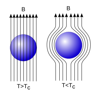
The Meissner effect is the expulsion of a magnetic field from a superconductor during its transition to the superconducting state when it is cooled below the critical temperature. This expulsion will repel a nearby magnet.
Pyroelectricity is a property of certain crystals which are naturally electrically polarized and as a result contain large electric fields. Pyroelectricity can be described as the ability of certain materials to generate a temporary voltage when they are heated or cooled. The change in temperature modifies the positions of the atoms slightly within the crystal structure, such that the polarization of the material changes. This polarization change gives rise to a voltage across the crystal. If the temperature stays constant at its new value, the pyroelectric voltage gradually disappears due to leakage current. The leakage can be due to electrons moving through the crystal, ions moving through the air, or current leaking through a voltmeter attached across the crystal.
The Schön scandal concerns German physicist Jan Hendrik Schön who briefly rose to prominence after a series of apparent breakthroughs with semiconductors that were later discovered to be fraudulent. Before he was exposed, Schön had received the Otto-Klung-Weberbank Prize for Physics and the Braunschweig Prize in 2001, as well as the Outstanding Young Investigator Award of the Materials Research Society in 2002, all of which were later rescinded.
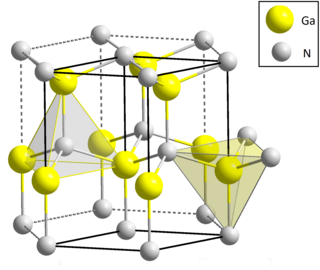
Gallium nitride is a binary III/V direct bandgap semiconductor commonly used in blue light-emitting diodes since the 1990s. The compound is a very hard material that has a Wurtzite crystal structure. Its wide band gap of 3.4 eV affords it special properties for applications in optoelectronic, high-power and high-frequency devices. For example, GaN is the substrate which makes violet (405 nm) laser diodes possible, without requiring nonlinear optical frequency-doubling.
The Kerr effect, also called the quadratic electro-optic (QEO) effect, is a change in the refractive index of a material in response to an applied electric field. The Kerr effect is distinct from the Pockels effect in that the induced index change is directly proportional to the square of the electric field instead of varying linearly with it. All materials show a Kerr effect, but certain liquids display it more strongly than others. The Kerr effect was discovered in 1875 by Scottish physicist John Kerr.

A metamaterial is any material engineered to have a property that is not found in naturally occurring materials. They are made from assemblies of multiple elements fashioned from composite materials such as metals and plastics. The materials are usually arranged in repeating patterns, at scales that are smaller than the wavelengths of the phenomena they influence. Metamaterials derive their properties not from the properties of the base materials, but from their newly designed structures. Their precise shape, geometry, size, orientation and arrangement gives them their smart properties capable of manipulating electromagnetic waves: by blocking, absorbing, enhancing, or bending waves, to achieve benefits that go beyond what is possible with conventional materials.
Smart materials, also called intelligent or responsive materials, are designed materials that have one or more properties that can be significantly changed in a controlled fashion by external stimuli, such as stress, moisture, electric or magnetic fields, light, temperature, pH, or chemical compounds. Smart materials are the basis of many applications, including sensors and actuators, or artificial muscles, particularly as electroactive polymers (EAPs).

Electrorheological (ER) fluids are suspensions of extremely fine non-conducting but electrically active particles in an electrically insulating fluid. The apparent viscosity of these fluids changes reversibly by an order of up to 100,000 in response to an electric field. For example, a typical ER fluid can go from the consistency of a liquid to that of a gel, and back, with response times on the order of milliseconds. The effect is sometimes called the Winslow effect after its discoverer, the American inventor Willis Winslow, who obtained a US patent on the effect in 1947 and wrote an article published in 1949.

Isamu Akasaki was a Japanese engineer and physicist, specializing in the field of semiconductor technology and Nobel Prize laureate, best known for inventing the bright gallium nitride (GaN) p-n junction blue LED in 1989 and subsequently the high-brightness GaN blue LED as well.
Shape-memory polymers (SMPs) are polymeric smart materials that have the ability to return from a deformed state to their original (permanent) shape when induced by an external stimulus (trigger), such as temperature change.
Photothermal spectroscopy is a group of high sensitivity spectroscopy techniques used to measure optical absorption and thermal characteristics of a sample. The basis of photothermal spectroscopy is the change in thermal state of the sample resulting from the absorption of radiation. Light absorbed and not lost by emission results in heating. The heat raises temperature thereby influencing the thermodynamic properties of the sample or of a suitable material adjacent to it. Measurement of the temperature, pressure, or density changes that occur due to optical absorption are ultimately the basis for the photothermal spectroscopic measurements.

An oxide thin-film transistor or metal oxide thin film transistor is a type of thin film transistor where the semiconductor is a metal oxide compound. An oxide TFT is distinct from a metal oxide field effect transistor (MOSFET) where the word "oxide" refers to the insulating gate dielectric. In an oxide TFT, the word oxide refers to the semiconductor. Oxide TFTs have applications as amplifiers to deliver current to emitters in display backplanes.
The photoacoustic effect or optoacoustic effect is the formation of sound waves following light absorption in a material sample. In order to obtain this effect the light intensity must vary, either periodically or as a single flash. The photoacoustic effect is quantified by measuring the formed sound with appropriate detectors, such as microphones or piezoelectric sensors. The time variation of the electric output from these detectors is the photoacoustic signal. These measurements are useful to determine certain properties of the studied sample. For example, in photoacoustic spectroscopy, the photoacoustic signal is used to obtain the actual absorption of light in either opaque or transparent objects. It is useful for substances in extremely low concentrations, because very strong pulses of light from a laser can be used to increase sensitivity and very narrow wavelengths can be used for specificity. Furthermore, photoacoustic measurements serve as a valuable research tool in the study of the heat evolved in photochemical reactions, particularly in the study of photosynthesis.

Hiroshi Amano is a Japanese physicist, engineer and inventor specializing in the field of semiconductor technology. For his work he was awarded the 2014 Nobel Prize in Physics together with Isamu Akasaki and Shuji Nakamura for "the invention of efficient blue light-emitting diodes which has enabled bright and energy-saving white light sources".

Kenji Uchino is an American electronics engineer, physicist, academic, inventor and industry executive. He is currently a Professor of Electrical Engineering at Pennsylvania State University, where he also directs the International Center for Actuators and Transducers at Materials Research Institute. He is the former Associate Director at The US Office of Naval Research – Global Tokyo Office.
References
- ↑ Bell, A. G. (1881). "On the Production and Reproduction of Sound by Light". Proceedings of the American Association for the Advancement of Science. 29: 115.
- ↑ Uchino, Kenji; Cross, Leslie E. (1980). "Electrostriction and Its Interrelation with Other Anharmonic Properties of Materials". Japanese Journal of Applied Physics. Japan Society of Applied Physics. 19 (4): L171–L173. Bibcode:1980JaJAP..19L.171U. doi:10.1143/jjap.19.l171. ISSN 0021-4922.