
Chemical vapor deposition (CVD) is a vacuum deposition method used to produce high-quality, and high-performance, solid materials. The process is often used in the semiconductor industry to produce thin films.

MEMS is the technology of microscopic devices incorporating both electronic and moving parts. MEMS are made up of components between 1 and 100 micrometres in size, and MEMS devices generally range in size from 20 micrometres to a millimetre, although components arranged in arrays can be more than 1000 mm2. They usually consist of a central unit that processes data and several components that interact with the surroundings.
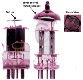
A getter is a deposit of reactive material that is placed inside a vacuum system to complete and maintain the vacuum. When gas molecules strike the getter material, they combine with it chemically or by absorption. Thus the getter removes small amounts of gas from the evacuated space. The getter is usually a coating applied to a surface within the evacuated chamber.

Pulsed laser deposition (PLD) is a physical vapor deposition (PVD) technique where a high-power pulsed laser beam is focused inside a vacuum chamber to strike a target of the material that is to be deposited. This material is vaporized from the target which deposits it as a thin film on a substrate. This process can occur in ultra high vacuum or in the presence of a background gas, such as oxygen which is commonly used when depositing oxides to fully oxygenate the deposited films.
A thin film is a layer of material ranging from fractions of a nanometer (monolayer) to several micrometers in thickness. The controlled synthesis of materials as thin films is a fundamental step in many applications. A familiar example is the household mirror, which typically has a thin metal coating on the back of a sheet of glass to form a reflective interface. The process of silvering was once commonly used to produce mirrors, while more recently the metal layer is deposited using techniques such as sputtering. Advances in thin film deposition techniques during the 20th century have enabled a wide range of technological breakthroughs in areas such as magnetic recording media, electronic semiconductor devices, integrated passive devices, light-emitting diodes, optical coatings, hard coatings on cutting tools, and for both energy generation and storage. It is also being applied to pharmaceuticals, via thin-film drug delivery. A stack of thin films is called a multilayer.
Titanium nitride is an extremely hard ceramic material, often used as a physical vapor deposition (PVD) coating on titanium alloys, steel, carbide, and aluminium components to improve the substrate's surface properties.

Zirconium nitride is an inorganic compound used in a variety of ways due to its properties.

Ion plating (IP) is a physical vapor deposition (PVD) process that is sometimes called ion assisted deposition (IAD) or ion vapor deposition (IVD) and is a modified version of vacuum deposition. Ion plating uses concurrent or periodic bombardment of the substrate, and deposits film by atomic-sized energetic particles called ions. Bombardment prior to deposition is used to sputter clean the substrate surface. During deposition the bombardment is used to modify and control the properties of the depositing film. It is important that the bombardment be continuous between the cleaning and the deposition portions of the process to maintain an atomically clean interface. If this interface is not properly cleaned, then it can result into a weaker coating or poor adhesion.

Nitriding is a heat treating process that diffuses nitrogen into the surface of a metal to create a case-hardened surface. These processes are most commonly used on low-alloy steels. They are also used on titanium, aluminium and molybdenum.
Electron-beam physical vapor deposition, or EBPVD, is a form of physical vapor deposition in which a target anode is bombarded with an electron beam given off by a charged tungsten filament under high vacuum. The electron beam causes atoms from the target to transform into the gaseous phase. These atoms then precipitate into solid form, coating everything in the vacuum chamber with a thin layer of the anode material.

Tantalum nitride (TaN) is a chemical compound, a nitride of tantalum. There are multiple phases of compounds, stoichimetrically from Ta2N to Ta3N5, including TaN.
Vacuum deposition is a group of processes used to deposit layers of material atom-by-atom or molecule-by-molecule on a solid surface. These processes operate at pressures well below atmospheric pressure. The deposited layers can range from a thickness of one atom up to millimeters, forming freestanding structures. Multiple layers of different materials can be used, for example to form optical coatings. The process can be qualified based on the vapor source; physical vapor deposition uses a liquid or solid source and chemical vapor deposition uses a chemical vapor.
Platit AG is a Swiss company that manufactures and markets coating equipment for the manufacturing cutting tool industry.

Plasma-enhanced chemical vapor deposition (PECVD) is a chemical vapor deposition process used to deposit thin films from a gas state (vapor) to a solid state on a substrate. Chemical reactions are involved in the process, which occur after creation of a plasma of the reacting gases. The plasma is generally created by radio frequency (RF) frequency or direct current (DC) discharge between two electrodes, the space between which is filled with the reacting gases.

Evaporation is a common method of thin-film deposition. The source material is evaporated in a vacuum. The vacuum allows vapor particles to travel directly to the target object (substrate), where they condense back to a solid state. Evaporation is used in microfabrication, and to make macro-scale products such as metallized plastic film.

Sputter deposition is a physical vapor deposition (PVD) method of thin film deposition by the phenomenon of sputtering. This involves ejecting material from a "target" that is a source onto a "substrate" such as a silicon wafer. Resputtering is re-emission of the deposited material during the deposition process by ion or atom bombardment. Sputtered atoms ejected from the target have a wide energy distribution, typically up to tens of eV. The sputtered ions can ballistically fly from the target in straight lines and impact energetically on the substrates or vacuum chamber. Alternatively, at higher gas pressures, the ions collide with the gas atoms that act as a moderator and move diffusively, reaching the substrates or vacuum chamber wall and condensing after undergoing a random walk. The entire range from high-energy ballistic impact to low-energy thermalized motion is accessible by changing the background gas pressure. The sputtering gas is often an inert gas such as argon. For efficient momentum transfer, the atomic weight of the sputtering gas should be close to the atomic weight of the target, so for sputtering light elements neon is preferable, while for heavy elements krypton or xenon are used. Reactive gases can also be used to sputter compounds. The compound can be formed on the target surface, in-flight or on the substrate depending on the process parameters. The availability of many parameters that control sputter deposition make it a complex process, but also allow experts a large degree of control over the growth and microstructure of the film.
Substrate is a term used in materials science and engineering to describe the base material on which processing is conducted. Surfaces have different uses, including producing new film or layers of material and being a base to which another substance is bonded.
High-power impulse magnetron sputtering is a method for physical vapor deposition of thin films which is based on magnetron sputter deposition. HIPIMS utilises extremely high power densities of the order of kW⋅cm−2 in short pulses (impulses) of tens of microseconds at low duty cycle of < 10%. Distinguishing features of HIPIMS are a high degree of ionisation of the sputtered metal and a high rate of molecular gas dissociation which result in high density of deposited films. The ionization and dissociation degree increase according to the peak cathode power. The limit is determined by the transition of the discharge from glow to arc phase. The peak power and the duty cycle are selected so as to maintain an average cathode power similar to conventional sputtering (1–10 W⋅cm−2).
Precision glass moulding is a replicative process that allows the production of high precision optical components from glass without grinding and polishing. The process is also known as ultra-precision glass pressing. It is used to manufacture precision glass lenses for consumer products such as digital cameras, and high-end products like medical systems. The main advantage over mechanical lens production is that complex lens geometries such as aspheres can be produced cost-efficiently.

Titanium aluminium nitride (TiAlN) or aluminium titanium nitride is a group of metastable hard coatings consisting of nitrogen and the metallic elements aluminium and titanium. This compound as well as similar compounds(such as TiN and TiCN) are most notably used for coating machine tools such and endmills and drills to change their properties, such as increased thermal stability and/or wear resistance. Four important compositions are deposited in industrial scale by physical vapor deposition methods:


