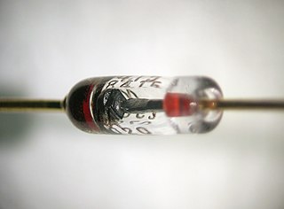
A diode is a two-terminal electronic component that conducts current primarily in one direction. It has low resistance in one direction and high resistance in the other.

Ion implantation is a low-temperature process by which ions of one element are accelerated into a solid target, thereby changing the physical, chemical, or electrical properties of the target. Ion implantation is used in semiconductor device fabrication and in metal finishing, as well as in materials science research. The ions can alter the elemental composition of the target if they stop and remain in the target. Ion implantation also causes chemical and physical changes when the ions impinge on the target at high energy. The crystal structure of the target can be damaged or even destroyed by the energetic collision cascades, and ions of sufficiently high energy can cause nuclear transmutation.

A triode is an electronic amplifying vacuum tube consisting of three electrodes inside an evacuated glass envelope: a heated filament or cathode, a grid, and a plate (anode). Developed from Lee De Forest's 1906 Audion, a partial vacuum tube that added a grid electrode to the thermionic diode, the triode was the first practical electronic amplifier and the ancestor of other types of vacuum tubes such as the tetrode and pentode. Its invention helped make amplified radio technology and long-distance telephony possible. Triodes were widely used in consumer electronics devices such as radios and televisions until the 1970s, when transistors replaced them. Today, their main remaining use is in high-power RF amplifiers in radio transmitters and industrial RF heating devices. In recent years there has been a resurgence in demand for low power triodes due to renewed interest in tube-type audio systems by audiophiles who prefer the sound of tube-based electronics.

A vacuum tube, electron tube, valve, or tube, is a device that controls electric current flow in a high vacuum between electrodes to which an electric potential difference has been applied.

A semiconductor device is an electronic component that relies on the electronic properties of a semiconductor material for its function. Its conductivity lies between conductors and insulators. Semiconductor devices have replaced vacuum tubes in most applications. They conduct electric current in the solid state, rather than as free electrons across a vacuum or as free electrons and ions through an ionized gas.
A Langmuir probe is a device used to determine the electron temperature, electron density, and electric potential of a plasma. It works by inserting one or more electrodes into a plasma, with a constant or time-varying electric potential between the various electrodes or between them and the surrounding vessel. The measured currents and potentials in this system allow the determination of the physical properties of the plasma.
A tetrode is a vacuum tube having four active electrodes. The four electrodes in order from the centre are: a thermionic cathode, first and second grids, and a plate. There are several varieties of tetrodes, the most common being the screen-grid tube and the beam tetrode. In screen-grid tubes and beam tetrodes, the first grid is the control grid and the second grid is the screen grid. In other tetrodes one of the grids is a control grid, while the other may have a variety of functions.

A thyratron is a type of gas-filled tube used as a high-power electrical switch and controlled rectifier. Thyratrons can handle much greater currents than similar hard-vacuum tubes. Electron multiplication occurs when the gas becomes ionized, producing a phenomenon known as a Townsend discharge. Gases used include mercury vapor, xenon, neon, and hydrogen. Unlike a vacuum tube (valve), a thyratron cannot be used to amplify signals linearly.
Reactive-ion etching (RIE) is an etching technology used in microfabrication. RIE is a type of dry etching which has different characteristics than wet etching. RIE uses chemically reactive plasma to remove material deposited on wafers. The plasma is generated under low pressure (vacuum) by an electromagnetic field. High-energy ions from the plasma attack the wafer surface and react with it.
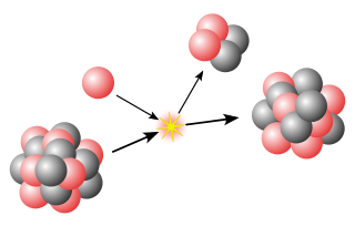
Neutron generators are neutron source devices which contain compact linear particle accelerators and that produce neutrons by fusing isotopes of hydrogen together. The fusion reactions take place in these devices by accelerating either deuterium, tritium, or a mixture of these two isotopes into a metal hydride target which also contains deuterium, tritium or a mixture of these isotopes. Fusion of deuterium atoms results in the formation of a helium-3 ion and a neutron with a kinetic energy of approximately 2.5 MeV. Fusion of a deuterium and a tritium atom results in the formation of a helium-4 ion and a neutron with a kinetic energy of approximately 14.1 MeV. Neutron generators have applications in medicine, security, and materials analysis.

An ion beam is a type of charged particle beam consisting of ions. Ion beams have many uses in electronics manufacturing and other industries. A variety of ion beam sources exists, some derived from the mercury vapor thrusters developed by NASA in the 1960s. The most common ion beams are of singly-charged ions.

A pentode is an electronic device having five electrodes. The term most commonly applies to a three-grid amplifying vacuum tube or thermionic valve that was invented by Gilles Holst and Bernhard D.H. Tellegen in 1926. The pentode was developed from the screen-grid tube or shield-grid tube by the addition of a grid between the screen grid and the plate. The screen-grid tube was limited in performance as an amplifier due to secondary emission of electrons from the plate. The additional grid is called the suppressor grid. The suppressor grid is usually operated at or near the potential of the cathode and prevents secondary emission electrons from the plate from reaching the screen grid. The addition of the suppressor grid permits much greater output signal amplitude to be obtained from the plate of the pentode in amplifier operation than from the plate of the screen-grid tube at the same plate supply voltage. Pentodes were widely manufactured and used in electronic equipment until the 1960s to 1970s, during which time transistors replaced tubes in new designs. During the first quarter of the 21st century, a few pentode tubes have been in production for high power radio frequency applications, musical instrument amplifiers, home audio and niche markets.

The hot-filament ionization gauge, sometimes called a hot-filament gauge or hot-cathode gauge, is the most widely used low-pressure (vacuum) measuring device for the region from 10−3 to 10−10 Torr. It is a triode, with the filament being the cathode.
A capacitively coupled plasma (CCP) is one of the most common types of industrial plasma sources. It essentially consists of two metal electrodes separated by a small distance, placed in a reactor. The gas pressure in the reactor can be lower than atmosphere or it can be atmospheric.

In the early days of electronics, devices that used vacuum tubes, such as radios, were powered by batteries. Each battery had a different designation depending on which tube element it was associated with.
Plasma etching is a form of plasma processing used to fabricate integrated circuits. It involves a high-speed stream of glow discharge (plasma) of an appropriate gas mixture being shot at a sample. The plasma source, known as etch species, can be either charged (ions) or neutral. During the process, the plasma generates volatile etch products at room temperature from the chemical reactions between the elements of the material etched and the reactive species generated by the plasma. Eventually the atoms of the shot element embed themselves at or just below the surface of the target, thus modifying the physical properties of the target.

Sputter deposition is a physical vapor deposition (PVD) method of thin film deposition by the phenomenon of sputtering. This involves ejecting material from a "target" that is a source onto a "substrate" such as a silicon wafer. Resputtering is re-emission of the deposited material during the deposition process by ion or atom bombardment. Sputtered atoms ejected from the target have a wide energy distribution, typically up to tens of eV. The sputtered ions can ballistically fly from the target in straight lines and impact energetically on the substrates or vacuum chamber. Alternatively, at higher gas pressures, the ions collide with the gas atoms that act as a moderator and move diffusively, reaching the substrates or vacuum chamber wall and condensing after undergoing a random walk. The entire range from high-energy ballistic impact to low-energy thermalized motion is accessible by changing the background gas pressure. The sputtering gas is often an inert gas such as argon. For efficient momentum transfer, the atomic weight of the sputtering gas should be close to the atomic weight of the target, so for sputtering light elements neon is preferable, while for heavy elements krypton or xenon are used. Reactive gases can also be used to sputter compounds. The compound can be formed on the target surface, in-flight or on the substrate depending on the process parameters. The availability of many parameters that control sputter deposition make it a complex process, but also allow experts a large degree of control over the growth and microstructure of the film.
The inductive output tube (IOT) or klystrode is a variety of linear-beam vacuum tube, similar to a klystron, used as a power amplifier for high frequency radio waves. It evolved in the 1980s to meet increasing efficiency requirements for high-power RF amplifiers in radio transmitters. The primary commercial use of IOTs is in UHF television transmitters, where they have mostly replaced klystrons because of their higher efficiencies and smaller size. IOTs are also used in particle accelerators. They are capable of producing power output up to about 30 kW continuous and 7 MW pulsed and gains of 20–23 dB at frequencies up to about a gigahertz.
Plasma-activated bonding is a derivative, directed to lower processing temperatures for direct bonding with hydrophilic surfaces. The main requirements for lowering temperatures of direct bonding are the use of materials melting at low temperatures and with different coefficients of thermal expansion (CTE).

