Validation
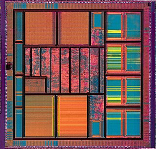
Chips comprising 500,000 logic elements are the silicon brains inside cell phones, MP3 players, computer printers and peripherals, digital television sets, medical imaging systems, components used in transportation safety and comfort, and even building management systems. Either because of their broad consumer proliferation, or because of their mission-critical application, the manufacturer must be absolutely certain that the device is thoroughly validated.
The best way to achieve high confidence is to leverage the pre-silicon verification work — which can comprise as much as 30% of the overall cost of the implementation — and use that knowledge in the post-silicon system. Today, much of this work is done manually, which partially explains the high costs associated with system validation. However, there are some tools that have been recently introduced to automate post-silicon system validation.
Observability
Simulation-based design environments enjoy the tremendous advantage of nearly perfect observability, meaning the designer can see any signal at nearly any time. They suffer, however, from the restricted amount of data they can generate during post-silicon system validation. Many complicated devices indicate their problems only after days or weeks of testing, and they produce a volume of data that would take centuries to reproduce on a simulator. FPGA-based emulators, a well-established part of most implementation techniques, are faster than software simulators but will not deliver the comprehensive at-system-speed tests needed for device reliability.
Moreover, the problem of post-silicon validation is getting worse, as design complexity increases because of the terrific advances in semiconductor materials processing. The duration from prototype silicon — so-called "first silicon" — to volume production is increasing, and bugs do escape to the customers. The expense associated with IP-hardening is increasing. The industry today is focused on techniques that allow designers to better amortize their investment in pre-silicon verification to post-silicon validation. The best of these solutions enable affordable, scalable, automated, on-chip wire-scale visibility.
Benefits
Post-silicon validation encompasses all that validation effort that is poured onto a system after the first few silicon prototypes become available, but before product release. While in the past most of this effort was dedicated to validating electrical aspects of the design, or diagnosing systematic manufacturing defects, today a growing portion of the effort focuses on functional system validation. This trend is for the most part due to the increasing complexity of digital systems, which limits the verification coverage provided by traditional pre-silicon methodologies. As a result, a number of functional bugs survive into manufactured silicon, and it is the job of post-silicon validation to detect and diagnose them so that they do not escape into the released system. The bugs in this category are often system-level bugs and rare corner-case situations buried deep in the design state space: since these problems encompass many design modules, they are difficult to identify with pre-silicon tools, characterized by limited scalability and performance.
Post-silicon validation, on the other hand, benefits from very high raw performance, since tests are executed directly on manufactured silicon. At the same time, it poses several challenges to traditional validation methodologies, because of the limited internal observability and difficulty of applying modifications to manufactured silicon chips. These two factors lead in turn to critical challenges in error diagnosis and correction.
Very large-scale integration (VLSI) is the process of creating an integrated circuit (IC) by combining millions of MOS transistors onto a single chip. VLSI began in the 1970s when MOS integrated circuit chips were widely adopted, enabling complex semiconductor and telecommunication technologies to be developed. The microprocessor and memory chips are VLSI devices. Before the introduction of VLSI technology, most ICs had a limited set of functions they could perform. An electronic circuit might consist of a CPU, ROM, RAM and other glue logic. VLSI lets IC designers add all of these into one chip.

Digital electronics is a field of electronics involving the study of digital signals and the engineering of devices that use or produce them. This is in contrast to analog electronics and analog signals.

A system on a chip is an integrated circuit that integrates all or most components of a computer or other electronic system. These components almost always include a central processing unit (CPU), memory, input/output ports and secondary storage, often alongside other components such as radio modems and a GPU – all on a single substrate or microchip. It may contain digital, analog, mixed-signal, and often radio frequency signal processing functions.

An application-specific integrated circuit is an integrated circuit (IC) chip customized for a particular use, rather than intended for general-purpose use. For example, a chip designed to run in a digital voice recorder or a high-efficiency bitcoin miner is an ASIC. Application-specific standard product (ASSP) chips are intermediate between ASICs and industry standard integrated circuits like the 7400 series or the 4000 series. ASIC chips are typically fabricated using metal-oxide-semiconductor (MOS) technology, as MOS integrated circuit chips.
Mentor Graphics is a US-based electronic design automation (EDA) multinational corporation for electrical engineering and electronics, headquartered in Wilsonville, Oregon. The company was acquired by Siemens in 2017 and is now known as Siemens EDA.
Electronic design automation (EDA), also referred to as electronic computer-aided design (ECAD), is a category of software tools for designing electronic systems such as integrated circuits and printed circuit boards. The tools work together in a design flow that chip designers use to design and analyze entire semiconductor chips. Since a modern semiconductor chip can have billions of components, EDA tools are essential for their design; this article in particular describes EDA specifically with respect to integrated circuits (ICs).
Synopsys is an American electronic design automation company that focuses on silicon design and verification, silicon intellectual property and software security and quality. Products include logic synthesis, behavioral synthesis, place and route, static timing analysis, formal verification, hardware description language simulators, and transistor-level circuit simulation. The simulators include development and debugging environments that assist in the design of the logic for chips and computer systems. In recent years, Synopsys has expanded its products and services to include application security testing. Their technology is present in self-driving cars, artificial intelligence, and internet of things consumer products.
JTAG is an industry standard for verifying designs and testing printed circuit boards after manufacture.

Silvaco Inc. develops and markets electronic design automation (EDA) and technology CAD (TCAD) software and semiconductor design IP (SIP). The company is headquartered in Santa Clara, California, and has a global presence with offices located in North America, Europe, and throughout Asia. Since its founding in 1984, Silvaco has grown to become a large privately held EDA company. The company has been known by at least two other names: Silvaco International, and Silvaco Data Systems.
In electronic design, a semiconductor intellectual property core, IP core, or IP block is a reusable unit of logic, cell, or integrated circuit layout design that is the intellectual property of one party. IP cores can be licensed to another party or owned and used by a single party. The term comes from the licensing of the patent or source code copyright that exists in the design. Designers of application-specific integrated circuits (ASIC) and systems of field-programmable gate array (FPGA) logic can use IP cores as building blocks.
Design for testing or design for testability (DFT) consists of IC design techniques that add testability features to a hardware product design. The added features make it easier to develop and apply manufacturing tests to the designed hardware. The purpose of manufacturing tests is to validate that the product hardware contains no manufacturing defects that could adversely affect the product's correct functioning.

Integrated circuit design, or IC design, is a subset of electronics engineering, encompassing the particular logic and circuit design techniques required to design integrated circuits, or ICs. ICs consist of miniaturized electronic components built into an electrical network on a monolithic semiconductor substrate by photolithography.
Logic simulation is the use of simulation software to predict the behavior of digital circuits and hardware description languages. Simulation can be performed at varying degrees of physical abstraction, such as at the transistor level, gate level, register-transfer level (RTL), electronic system-level (ESL), or behavioral level.

In integrated circuit design, hardware emulation is the process of imitating the behavior of one or more pieces of hardware with another piece of hardware, typically a special purpose emulation system. The emulation model is usually based on a hardware description language source code, which is compiled into the format used by emulation system. The goal is normally debugging and functional verification of the system being designed. Often an emulator is fast enough to be plugged into a working target system in place of a yet-to-be-built chip, so the whole system can be debugged with live data. This is a specific case of in-circuit emulation.
Electronic system level (ESL) design and verification is an electronic design methodology, focused on higher abstraction level concerns. The term Electronic System Level or ESL Design was first defined by Gartner Dataquest, an EDA-industry-analysis firm, on February 1, 2001. It is defined in ESL Design and Verification as: "the utilization of appropriate abstractions in order to increase comprehension about a system, and to enhance the probability of a successful implementation of functionality in a cost-effective manner."
Aldec, Inc. is a privately owned electronic design automation company based in Henderson, Nevada that provides software and hardware used in creation and verification of digital designs targeting FPGA and ASIC technologies.
DAFCA, Inc. was an EDA software company focused on post-silicon validation, debug, and in-system bring-up of integrated circuits. DAFCA's tools allow design teams to incorporate patented and compact reconfigurable instrumentation IP into their devices, pre-silicon, in order to observe, discover, and diagnose at-speed, in-silicon functional behavior.
IC Manage is a company that provides design data and IP management, Big Data Analytics, Hybrid Cloud Bursting, and High-Performance Computing software to semiconductors, systems, Internet of Things and artificial intelligence IC companies.
In the electronics industry, embedded instrumentation refers to the integration of test and measurement instrumentation into semiconductor chips. Embedded instrumentation differs from embedded system, which are electronic systems or subsystems that usually comprise the control portion of a larger electronic system. Instrumentation embedded into chips is employed in a variety of electronic test applications, including validating and testing chips themselves, validating, testing and debugging the circuit boards where these chips are deployed, and troubleshooting systems once they have been installed in the field.

Vivado Design Suite is a software suite produced by Xilinx for synthesis and analysis of HDL designs, superseding Xilinx ISE with additional features for system on a chip development and high-level synthesis. Vivado represents a ground-up rewrite and re-thinking of the entire design flow.