Software focuses
This article may be too technical for most readers to understand.(February 2017) |
Design
Design flow primarily remains characterised via several primary components; these include:
- High-level synthesis (additionally known as behavioral synthesis or algorithmic synthesis) – The high-level design description (e.g. in C/C++) is converted into RTL or the register transfer level, responsible for representing circuitry via the utilisation of interactions between registers.
- Logic synthesis – The translation of RTL design description (e.g. written in Verilog or VHDL) into a discrete netlist or representation of logic gates.
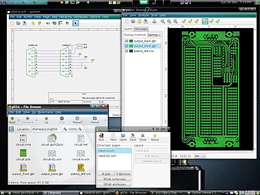
- Schematic capture – For standard cell digital, analog, RF-like Capture CIS in Orcad by Cadence and ISIS in Proteus.[ clarification needed ]
- Layout – usually schematic-driven layout, like Layout in Orcad by Cadence, ARES in Proteus
Simulation
- Transistor simulation – low-level transistor-simulation of a schematic/layout's behavior, accurate at device-level.
- Logic simulation – digital-simulation of an RTL or gate-netlist's digital (Boolean 0/1) behavior, accurate at Boolean-level.
- Behavioral simulation – high-level simulation of a design's architectural operation, accurate at cycle-level or interface-level.
- Hardware emulation – Use of special purpose hardware to emulate the logic of a proposed design. Can sometimes be plugged into a system in place of a yet-to-be-built chip; this is called in-circuit emulation .
- Technology CAD simulate and analyze the underlying process technology. Electrical properties of devices are derived directly from device physics

Analysis and verification
- Functional verification: ensures logic design matches specifications and executes tasks correctly. Includes dynamic functional verification via simulation, emulation, and prototypes. [11]
- RTL Linting for adherence to coding rules such as syntax, semantics, and style. [12]
- Clock domain crossing verification (CDC check): similar to linting, but these checks/tools specialize in detecting and reporting potential issues like data loss, meta-stability due to use of multiple clock domains in the design.
- Formal verification, also model checking: attempts to prove, by mathematical methods, that the system has certain desired properties, and that some undesired effects (such as deadlock) cannot occur.
- Equivalence checking: algorithmic comparison between a chip's RTL-description and synthesized gate-netlist, to ensure functional equivalence at the logical level.
- Static timing analysis: analysis of the timing of a circuit in an input-independent manner, hence finding a worst case over all possible inputs.
- Layout extraction: starting with a proposed layout, compute the (approximate) electrical characteristics of every wire and device. Often used in conjunction with static timing analysis above to estimate the performance of the completed chip.
- Electromagnetic field solvers, or just field solvers, solve Maxwell's equations directly for cases of interest in IC and PCB design. They are known for being slower but more accurate than the layout extraction above.
- Physical verification, PV: checking if a design is physically manufacturable, and that the resulting chips will not have any function-preventing physical defects, and will meet original specifications.
Manufacturing preparation
- Mask data preparation or MDP - The generation of actual lithography photomasks, utilised to physically manufacture the chip.
- Chip finishing which includes custom designations and structures to improve manufacturability of the layout. Examples of the latter are a seal ring and filler structures. [13]
- Producing a reticle layout with test patterns and alignment marks.
- Layout-to-mask preparation that enhances layout data with graphics operations, such as resolution enhancement techniques (RET) – methods for increasing the quality of the final photomask. This also includes optical proximity correction (OPC) or inverse lithography technology (ILT) – the up-front compensation for diffraction and interference effects occurring later when chip is manufactured using this mask.
- Mask generation – The generation of flat mask image from hierarchical design.
- Automatic test pattern generation or ATPG – The generation of pattern data systematically to exercise as many logic-gates and other components as possible.
- Built-in self-test or BIST – The installation of self-contained test-controllers to automatically test a logic or memory structure in the design
Functional safety
- Functional safety analysis, systematic computation of failure in time (FIT) rates and diagnostic coverage metrics for designs in order to meet the compliance requirements for the desired safety integrity levels.
- Functional safety synthesis, add reliability enhancements to structured elements (modules, RAMs, ROMs, register files, FIFOs) to improve fault detection / fault tolerance. This includes (not limited to) addition of error detection and / or correction codes (Hamming), redundant logic for fault detection and fault tolerance (duplicate / triplicate) and protocol checks (interface parity, address alignment, beat count)
- Functional safety verification, running of a fault campaign, including insertion of faults into the design and verification that the safety mechanism reacts in an appropriate manner for the faults that are deemed covered.