MMIX is a 64-bit reduced instruction set computing (RISC) architecture designed by Donald Knuth, with significant contributions by John L. Hennessy and Richard L. Sites. Knuth has said that,
MMIX is a computer intended to illustrate machine-level aspects of programming. In my books The Art of Computer Programming, it replaces MIX, the 1960s-style machine that formerly played such a role… I strove to design MMIX so that its machine language would be simple, elegant, and easy to learn. At the same time I was careful to include all of the complexities needed to achieve high performance in practice, so that MMIX could in principle be built and even perhaps be competitive with some of the fastest general-purpose computers in the marketplace."
In computer engineering, a reduced instruction set computer (RISC) is a computer designed to simplify the individual instructions given to the computer to accomplish tasks. Compared to the instructions given to a complex instruction set computer (CISC), a RISC computer might require more instructions in order to accomplish a task because the individual instructions are written in simpler code. The goal is to offset the need to process more instructions by increasing the speed of each instruction, in particular by implementing an instruction pipeline, which may be simpler given simpler instructions.

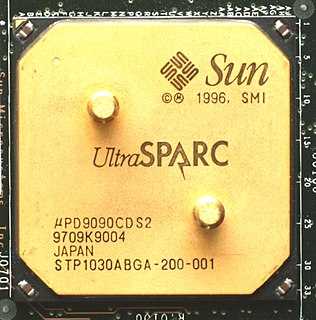
SPARC is a reduced instruction set computer (RISC) instruction set architecture originally developed by Sun Microsystems. Its design was strongly influenced by the experimental Berkeley RISC system developed in the early 1980s. First developed in 1986 and released in 1987, SPARC was one of the most successful early commercial RISC systems, and its success led to the introduction of similar RISC designs from many vendors through the 1980s and 90s.
In computer science, an instruction set architecture (ISA), also called computer architecture, is an abstract model of a computer. A device that executes instructions described by that ISA, such as a central processing unit (CPU), is called an implementation.
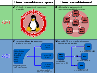
In computer software, an application binary interface (ABI) is an interface between two binary program modules. Often, one of these modules is a library or operating system facility, and the other is a program that is being run by a user.
In computer architecture, 64-bit integers, memory addresses, or other data units are those that are 64-bit (8-octet) wide. Also, 64-bit central processing unit (CPU) and arithmetic logic unit (ALU) architectures are those that are based on processor registers, address buses, or data buses of that size. 64-bit microcomputers are computers in which 64-bit microprocessors are the norm. From the software perspective, 64-bit computing means the use of machine code with 64-bit virtual memory addresses. However, not all 64-bit instruction sets support full 64-bit virtual memory addresses; x86-64 and ARMv8, for example, support only 48 bits of virtual address, with the remaining 16 bits of the virtual address required to be all 0's or all 1's, and several 64-bit instruction sets support fewer than 64 bits of physical memory address.
In computing, binary translation is a form of binary recompilation where sequences of instructions are translated from a source instruction set to the target instruction set. In some cases such as instruction set simulation, the target instruction set may be the same as the source instruction set, providing testing and debugging features such as instruction trace, conditional breakpoints and hot spot detection.
In computing, especially digital signal processing, the multiply–accumulate (MAC) or multiply-add (MAD) operation is a common step that computes the product of two numbers and adds that product to an accumulator. The hardware unit that performs the operation is known as a multiplier–accumulator ; the operation itself is also often called a MAC or a MAD operation. The MAC operation modifies an accumulator a:
Pyramid Technology Corporation was a computer company that produced a number of RISC-based minicomputers at the upper end of the performance range. It was based in the San Francisco Bay Area of California
The DLX is a RISC processor architecture designed by John L. Hennessy and David A. Patterson, the principal designers of the Stanford MIPS and the Berkeley RISC designs (respectively), the two benchmark examples of RISC design.

PRISM was a 32-bit RISC instruction set architecture (ISA) developed by Digital Equipment Corporation (DEC). It was the outcome of a number of DEC research projects from the 1982–1985 time-frame, and the project was subject to continually changing requirements and planned uses that delayed its introduction. This process eventually decided to use the design for a new line of Unix workstations. The arithmetic logic unit (ALU) of the microPrism version had completed design in April 1988 and samples were fabricated, but the design of other components like the floating point unit (FPU) and memory management unit (MMU) were still not complete in the summer when DEC management decided to cancel the project in favor of MIPS-based systems. An operating system codenamed MICA was developed for the PRISM architecture, which would have served as a replacement for both VAX/VMS and ULTRIX on PRISM.
Memory protection is a way to control memory access rights on a computer, and is a part of most modern instruction set architectures and operating systems. The main purpose of memory protection is to prevent a process from accessing memory that has not been allocated to it. This prevents a bug or malware within a process from affecting other processes, or the operating system itself. Protection may encompass all accesses to a specified area of memory, write accesses, or attempts to execute the contents of the area. An attempt to access unauthorized memory results in a hardware fault, e.g., a segmentation fault, storage violation exception, generally causing abnormal termination of the offending process. Memory protection for computer security includes additional techniques such as address space layout randomization and executable space protection.
A link register is a special-purpose register which holds the address to return to when a function call completes. This is more efficient than the more traditional scheme of storing return addresses on a call stack, sometimes called a machine stack. The link register does not require the writes and reads of the memory containing the stack which can save a considerable percentage of execution time with repeated calls of small subroutines.

The AMD Am29000, commonly shortened to 29k, is a family of 32-bit RISC microprocessors and microcontrollers developed and fabricated by Advanced Micro Devices (AMD). Based on the seminal Berkeley RISC, the 29k added a number of significant improvements. They were, for a time, the most popular RISC chips on the market, widely used in laser printers from a variety of manufacturers.
Berkeley RISC is one of two seminal research projects into reduced instruction set computer (RISC) based microprocessor design taking place under the Defense Advanced Research Projects Agency Very Large Scale Integration (VLSI) VLSI Project. RISC was led by David Patterson at the University of California, Berkeley between 1980 and 1984. The other project took place a short distance away at Stanford University under their MIPS effort starting in 1981 and running until 1984.
In computer science, a calling convention is an implementation-level (low-level) scheme for how subroutines receive parameters from their caller and how they return a result. Differences in various implementations include where parameters, return values, return addresses and scope links are placed, and how the tasks of preparing for a function call and restoring the environment afterwards are divided between the caller and the callee.
An instruction set architecture (ISA) is an abstract model of a computer, also referred to as computer architecture. A realization of an ISA is called an implementation. An ISA permits multiple implementations that may vary in performance, physical size, and monetary cost ; because the ISA serves as the interface between software and hardware. Software that has been written for an ISA can run on different implementations of the same ISA. This has enabled binary compatibility between different generations of computers to be easily achieved, and the development of computer families. Both of these developments have helped to lower the cost of computers and to increase their applicability. For these reasons, the ISA is one of the most important abstractions in computing today.
In computer programming, a subroutine is a sequence of program instructions that performs a specific task, packaged as a unit. This unit can then be used in programs wherever that particular task should be performed.
Since 1985, many processors implementing some version of the MIPS architecture have been designed and used widely.
