Related Research Articles
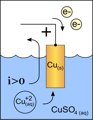
A cathode is the electrode from which a conventional current leaves a polarized electrical device. This definition can be recalled by using the mnemonic CCD for Cathode Current Departs. A conventional current describes the direction in which positive charges move. Electrons have a negative electrical charge, so the movement of electrons is opposite to that of the conventional current flow. Consequently, the mnemonic cathode current departs also means that electrons flow into the device's cathode from the external circuit. For example, the end of a household battery marked with a + (plus) is the cathode.
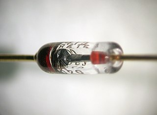
A diode is a two-terminal electronic component that conducts current primarily in one direction. It has low resistance in one direction and high resistance in the other.

A semiconductor device is an electronic component that relies on the electronic properties of a semiconductor material for its function. Its conductivity lies between conductors and insulators. Semiconductor devices have replaced vacuum tubes in most applications. They conduct electric current in the solid state, rather than as free electrons across a vacuum or as free electrons and ions through an ionized gas.

The junction field-effect transistor (JFET) is one of the simplest types of field-effect transistor. JFETs are three-terminal semiconductor devices that can be used as electronically controlled switches or resistors, or to build amplifiers.
A PIN diode is a diode with a wide, undoped intrinsic semiconductor region between a p-type semiconductor and an n-type semiconductor region. The p-type and n-type regions are typically heavily doped because they are used for ohmic contacts.
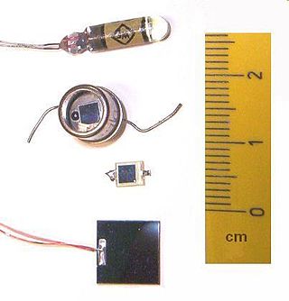
A photodiode is a semiconductor diode sensitive to photon radiation, such as visible light, infrared or ultraviolet radiation, X-rays and gamma rays. It produces an electrical current when it absorbs photons. This can be used for detection and measurement applications, or for the generation of electrical power in solar cells. Photodiodes are used in a wide range of applications throughout the electromagnetic spectrum from visible light photocells to gamma ray spectrometers.

A bipolar junction transistor (BJT) is a type of transistor that uses both electrons and electron holes as charge carriers. In contrast, a unipolar transistor, such as a field-effect transistor (FET), uses only one kind of charge carrier. A bipolar transistor allows a small current injected at one of its terminals to control a much larger current flowing between the terminals, making the device capable of amplification or switching.

A Zener diode is a special type of diode designed to reliably allow current to flow "backwards" when a certain set reverse voltage, known as the Zener voltage, is reached.

The Schottky diode, also known as Schottky barrier diode or hot-carrier diode, is a semiconductor diode formed by the junction of a semiconductor with a metal. It has a low forward voltage drop and a very fast switching action. The cat's-whisker detectors used in the early days of wireless and metal rectifiers used in early power applications can be considered primitive Schottky diodes.

A Schottky barrier, named after Walter H. Schottky, is a potential energy barrier for electrons formed at a metal–semiconductor junction. Schottky barriers have rectifying characteristics, suitable for use as a diode. One of the primary characteristics of a Schottky barrier is the Schottky barrier height, denoted by ΦB. The value of ΦB depends on the combination of metal and semiconductor.

A p–n junction is a boundary or interface between two types of semiconductor materials, p-type and n-type, inside a single crystal of semiconductor. The "p" (positive) side contains an excess of holes, while the "n" (negative) side contains an excess of electrons in the outer shells of the electrically neutral atoms there. This allows electric current to pass through the junction only in one direction. The p- and n-type regions creating the junction are made by doping the semiconductor, for example by ion implantation, diffusion of dopants, or by epitaxy.
A power semiconductor device is a semiconductor device used as a switch or rectifier in power electronics. Such a device is also called a power device or, when used in an integrated circuit, a power IC.
Deep-level transient spectroscopy (DLTS) is an experimental tool for studying electrically active defects in semiconductors. DLTS establishes fundamental defect parameters and measures their concentration in the material. Some of the parameters are considered as defect "finger prints" used for their identifications and analysis.
The saturation current, more accurately the reverse saturation current, is the part of the reverse current in a semiconductor diode caused by diffusion of minority carriers from the neutral regions to the depletion region. This current is almost independent of the reverse voltage.
In semiconductor physics, the depletion region, also called depletion layer, depletion zone, junction region, space charge region, or space charge layer, is an insulating region within a conductive, doped semiconductor material where the mobile charge carriers have diffused away, or forced away by an electric field. The only elements left in the depletion region are ionized donor or acceptor impurities. This region of uncovered positive and negative ions is called the depletion region due to the depletion of carriers in this region, leaving none to carry a current. Understanding the depletion region is key to explaining modern semiconductor electronics: diodes, bipolar junction transistors, field-effect transistors, and variable capacitance diodes all rely on depletion region phenomena.
In electronics, leakage is the gradual transfer of electrical energy across a boundary normally viewed as insulating, such as the spontaneous discharge of a charged capacitor, magnetic coupling of a transformer with other components, or flow of current across a transistor in the "off" state or a reverse-polarized diode.

The theory of solar cells explains the process by which light energy in photons is converted into electric current when the photons strike a suitable semiconductor device. The theoretical studies are of practical use because they predict the fundamental limits of a solar cell, and give guidance on the phenomena that contribute to losses and solar cell efficiency.

In electronics, the Zener effect is a type of electrical breakdown, discovered by Clarence Melvin Zener. It occurs in a reverse biased p-n diode when the electric field enables tunneling of electrons from the valence to the conduction band of a semiconductor, leading to numerous free minority carriers which suddenly increase the reverse current.
This article provides a more detailed explanation of p–n diode behavior than is found in the articles p–n junction or diode.
In solid-state physics, band bending refers to the process in which the electronic band structure in a material curves up or down near a junction or interface. It does not involve any physical (spatial) bending. When the electrochemical potential of the free charge carriers around an interface of a semiconductor is dissimilar, charge carriers are transferred between the two materials until an equilibrium state is reached whereby the potential difference vanishes. The band bending concept was first developed in 1938 when Mott, Davidov and Schottky all published theories of the rectifying effect of metal-semiconductor contacts. The use of semiconductor junctions sparked the computer revolution in 1990. Devices such as the diode, the transistor, the photocell and many more still play an important role in technology.
References
- ↑ Grob, Bernard (2000). Basic electronics (8. ed.). New York: Glencoe/McGraw-Hill. ISBN 002802253X.
- ↑ Floyd, Thomas L. (1999). Electronic devices (5. ed.). Upper Saddle River, NJ: Prentice Hall. ISBN 0136491383.
| | This electronics-related article is a stub. You can help Wikipedia by expanding it. |