
Gallium arsenide (GaAs) is a III-V direct band gap semiconductor with a zinc blende crystal structure.
In physical chemistry and engineering, passivation is coating a material so that it becomes "passive", that is, less readily affected or corroded by the environment. Passivation involves creation of an outer layer of shield material that is applied as a microcoating, created by chemical reaction with the base material, or allowed to build by spontaneous oxidation in the air. As a technique, passivation is the use of a light coat of a protective material, such as metal oxide, to create a shield against corrosion. Passivation of silicon is used during fabrication of microelectronic devices. Undesired passivation of electrodes, called "fouling", increases the circuit resistance so it interferes with some electrochemical applications such as electrocoagulation for wastewater treatment, amperometric chemical sensing, and electrochemical synthesis.

A Schottky barrier, named after Walter H. Schottky, is a potential energy barrier for electrons formed at a metal–semiconductor junction. Schottky barriers have rectifying characteristics, suitable for use as a diode. One of the primary characteristics of a Schottky barrier is the Schottky barrier height, denoted by ΦB. The value of ΦB depends on the combination of metal and semiconductor.
A heterojunction is an interface between two layers or regions of dissimilar semiconductors. These semiconducting materials have unequal band gaps as opposed to a homojunction. It is often advantageous to engineer the electronic energy bands in many solid-state device applications, including semiconductor lasers, solar cells and transistors. The combination of multiple heterojunctions together in a device is called a heterostructure, although the two terms are commonly used interchangeably. The requirement that each material be a semiconductor with unequal band gaps is somewhat loose, especially on small length scales, where electronic properties depend on spatial properties. A more modern definition of heterojunction is the interface between any two solid-state materials, including crystalline and amorphous structures of metallic, insulating, fast ion conductor and semiconducting materials.
A "photoelectrochemical cell" is one of two distinct classes of device. The first produces electrical energy similarly to a dye-sensitized photovoltaic cell, which meets the standard definition of a photovoltaic cell. The second is a photoelectrolytic cell, that is, a device which uses light incident on a photosensitizer, semiconductor, or aqueous metal immersed in an electrolytic solution to directly cause a chemical reaction, for example to produce hydrogen via the electrolysis of water.

A metal rectifier is an early type of semiconductor rectifier in which the semiconductor is copper oxide, germanium or selenium. They were used in power applications to convert alternating current to direct current in devices such as radios and battery chargers. Westinghouse Electric was a major manufacturer of these rectifiers since the late 1920s, under the trade name Westector.

Photodetectors, also called photosensors, are sensors of light or other electromagnetic radiation. There are a wide variety of photodetectors which may be classified by mechanism of detection, such as photoelectric or photochemical effects, or by various performance metrics, such as spectral response. Semiconductor-based photodetectors typically use a p–n junction that converts photons into charge. The absorbed photons make electron–hole pairs in the depletion region. Photodiodes and photo transistors are a few examples of photo detectors. Solar cells convert some of the light energy absorbed into electrical energy.

A dye-sensitized solar cell is a low-cost solar cell belonging to the group of thin film solar cells. It is based on a semiconductor formed between a photo-sensitized anode and an electrolyte, a photoelectrochemical system. The modern version of a dye solar cell, also known as the Grätzel cell, was originally co-invented in 1988 by Brian O'Regan and Michael Grätzel at UC Berkeley and this work was later developed by the aforementioned scientists at the École Polytechnique Fédérale de Lausanne (EPFL) until the publication of the first high efficiency DSSC in 1991. Michael Grätzel has been awarded the 2010 Millennium Technology Prize for this invention.

A solar cell or photovoltaic cell is an electronic device that converts the energy of light directly into electricity by means of the photovoltaic effect. It is a form of photoelectric cell, a device whose electrical characteristics vary when exposed to light. Individual solar cell devices are often the electrical building blocks of photovoltaic modules, known colloquially as "solar panels". The common single-junction silicon solar cell can produce a maximum open-circuit voltage of approximately 0.5 to 0.6 volts.
Hybrid solar cells combine advantages of both organic and inorganic semiconductors. Hybrid photovoltaics have organic materials that consist of conjugated polymers that absorb light as the donor and transport holes. Inorganic materials in hybrid cells are used as the acceptor and electron transporter in the structure. The hybrid photovoltaic devices have a potential for not only low-cost by roll-to-roll processing but also for scalable solar power conversion.

A quantum dot solar cell (QDSC) is a solar cell design that uses quantum dots as the captivating photovoltaic material. It attempts to replace bulk materials such as silicon, copper indium gallium selenide (CIGS) or cadmium telluride (CdTe). Quantum dots have bandgaps that are adjustable across a wide range of energy levels by changing their size. In bulk materials, the bandgap is fixed by the choice of material(s). This property makes quantum dots attractive for multi-junction solar cells, where a variety of materials are used to improve efficiency by harvesting multiple portions of the solar spectrum.
Third-generation photovoltaic cells are solar cells that are potentially able to overcome the Shockley–Queisser limit of 31–41% power efficiency for single bandgap solar cells. This includes a range of alternatives to cells made of semiconducting p-n junctions and thin film cells. Common third-generation systems include multi-layer ("tandem") cells made of amorphous silicon or gallium arsenide, while more theoretical developments include frequency conversion,, hot-carrier effects and other multiple-carrier ejection techniques.

Multi-junction (MJ) solar cells are solar cells with multiple p–n junctions made of different semiconductor materials. Each material's p-n junction will produce electric current in response to different wavelengths of light. The use of multiple semiconducting materials allows the absorbance of a broader range of wavelengths, improving the cell's sunlight to electrical energy conversion efficiency.
Organic photovoltaic devices (OPVs) are fabricated from thin films of organic semiconductors, such as polymers and small-molecule compounds, and are typically on the order of 100 nm thick. Because polymer based OPVs can be made using a coating process such as spin coating or inkjet printing, they are an attractive option for inexpensively covering large areas as well as flexible plastic surfaces. A promising low cost alternative to conventional solar cells made of crystalline silicon, there is a large amount of research being dedicated throughout industry and academia towards developing OPVs and increasing their power conversion efficiency.
An organic solar cell (OSC) or plastic solar cell is a type of photovoltaic that uses organic electronics, a branch of electronics that deals with conductive organic polymers or small organic molecules, for light absorption and charge transport to produce electricity from sunlight by the photovoltaic effect. Most organic photovoltaic cells are polymer solar cells.

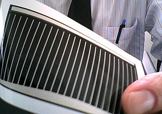
Thin-film solar cells are made by depositing one or more thin layers of photovoltaic material onto a substrate, such as glass, plastic or metal. Thin-film solar cells are typically a few nanometers (nm) to a few microns (µm) thick–much thinner than the wafers used in conventional crystalline silicon (c-Si) based solar cells, which can be up to 200 µm thick. Thin-film solar cells are commercially used in several technologies, including cadmium telluride (CdTe), copper indium gallium diselenide (CIGS), and amorphous thin-film silicon.
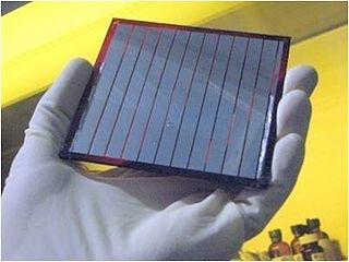
A copper indium gallium selenide solar cell is a thin-film solar cell used to convert sunlight into electric power. It is manufactured by depositing a thin layer of copper indium gallium selenide solid solution on glass or plastic backing, along with electrodes on the front and back to collect current. Because the material has a high absorption coefficient and strongly absorbs sunlight, a much thinner film is required than of other semiconductor materials.

Crystalline silicon or (c-Si) Is the crystalline forms of silicon, either polycrystalline silicon, or monocrystalline silicon. Crystalline silicon is the dominant semiconducting material used in photovoltaic technology for the production of solar cells. These cells are assembled into solar panels as part of a photovoltaic system to generate solar power from sunlight.
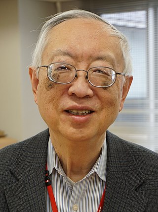
Robert P. H. Chang is an American materials scientist who served as the president of the Materials Research Society (1989) and as a general secretary and president of the International Union of Materials Research Societies (IUMRS). Currently Chang heads the Materials Research Institute at Northwestern University. He is a member of advisory boards of the National Institute for Materials Science and of the journal Science and Technology of Advanced Materials.

Heterojunction solar cells (HJT), variously known as Silicon heterojunctions (SHJ) or Heterojunction with Intrinsic Thin Layer (HIT), are a family of photovoltaic cell technologies based on a heterojunction formed between semiconductors with dissimilar band gaps. They are a hybrid technology, combining aspects of conventional crystalline solar cells with thin-film solar cells.
