The Intel 486, officially named i486 and also known as 80486, is a microprocessor. It is a higher-performance follow-up to the Intel 386. The i486 was introduced in 1989. It represents the fourth generation of binary compatible CPUs following the 8086 of 1978, the Intel 80286 of 1982, and 1985's i386.

The i486SX was a microprocessor originally released by Intel in 1991. It was a modified Intel i486DX microprocessor with its floating-point unit (FPU) disabled. It was intended as a lower-cost CPU for use in low-end systems, adapting the SX suffix of the earlier i386SX in order to connote a lower-cost option. However, unlike the i386SX, which had a 16-bit external data bus and a 24-bit external address bus, the i486SX was entirely 32-bit.

IntelDX4 is a clock-tripled i486 microprocessor with 16 KB level 1 cache. Intel named it DX4 as a consequence of litigation with AMD over trademarks. The product was officially named IntelDX4, but OEMs continued using the i486 naming convention.

The K6 microprocessor was launched by AMD in 1997. The main advantage of this particular microprocessor is that it was designed to fit into existing desktop designs for Pentium-branded CPUs. It was marketed as a product that could perform as well as its Intel Pentium II equivalent but at a significantly lower price. The K6 had a considerable impact on the PC market and presented Intel with serious competition.

The Pentium is a fifth generation, 32-bit x86 microprocessor that was introduced by Intel on March 22, 1993, as the very first CPU in the Pentium brand. It was instruction set compatible with the 80486 but was a new and very different microarchitecture design from previous iterations. The P5 Pentium was the first superscalar x86 microarchitecture and the world's first superscalar microprocessor to be in mass production—meaning it generally executes at least 2 instructions per clock mainly because of a design-first dual integer pipeline design previously thought impossible to implement on a CISC microarchitecture. Additional features include a faster floating-point unit, wider data bus, separate code and data caches, and many other techniques and features to enhance performance and support security, encryption, and multiprocessing, for workstations and servers when compared to the next best previous industry standard processor implementation before it, the Intel 80486.

Cyrix Corporation was a microprocessor developer that was founded in 1988 in Richardson, Texas, as a specialist supplier of floating point units for 286 and 386 microprocessors. The company was founded by Tom Brightman and Jerry Rogers.

The Am5x86 processor is an x86-compatible CPU announced in November of 1995 by AMD for use in 486-class computer systems. It began shipping in December of 1995, with a base price of $93 per unit in bulk quantities. Before being released, it was in development under the codename "X5".
The Pentium OverDrive was a microprocessor marketing brand name used by Intel, to cover a variety of consumer upgrade products sold in the mid-1990s. It was originally released for 486 motherboards, and later some Pentium sockets. Intel dropped the brand, as it failed to appeal to corporate buyers, and discouraged new system sales.

Socket 7 is a physical and electrical specification for an x86-style CPU socket on a personal computer motherboard. It was released in June 1995. The socket supersedes the earlier Socket 5, and accepts P5 Pentium microprocessors manufactured by Intel, as well as compatibles made by Cyrix/IBM, AMD, IDT and others. Socket 7 was the only socket that supported a wide range of CPUs from different manufacturers and a wide range of speeds.

A pin grid array (PGA) is a type of integrated circuit packaging. In a PGA, the package is square or rectangular, and the pins are arranged in a regular array on the underside of the package. The pins are commonly spaced 2.54 mm (0.1") apart, and may or may not cover the entire underside of the package.

In computer hardware, a CPU socket or CPU slot contains one or more mechanical components providing mechanical and electrical connections between a microprocessor and a printed circuit board (PCB). This allows for placing and replacing the central processing unit (CPU) without soldering.
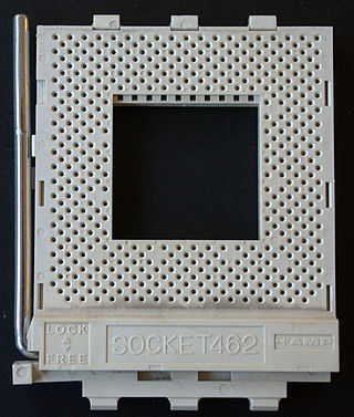
Socket A is a zero insertion force pin grid array (PGA) CPU socket used for AMD processors ranging from the Athlon Thunderbird to the Athlon XP/MP 3200+, and AMD budget processors including the Duron and Sempron. Socket A also supports AMD Geode NX embedded processors. The socket is a zero insertion force pin grid array type with 462 pins. The front-side bus frequencies supported for the AMD Athlon XP and Sempron are 133 MHz, 166 MHz, and 200 MHz. Socket A supports 32-bit CPUs only.

The land grid array (LGA) is a type of surface-mount packaging for integrated circuits (ICs) that is notable for having the pins on the socket — as opposed to pins on the integrated circuit, known as a pin grid array (PGA). An LGA can be electrically connected to a printed circuit board (PCB) either by the use of a socket or by soldering directly to the board.

Socket 479 (mPGA479M) is the CPU socket for the Intel Pentium M and Celeron M mobile processors normally used in laptops, but has also been used with Tualatin-M Pentium III processors. The official naming by Intel is µFCPGA and µPGA479M.
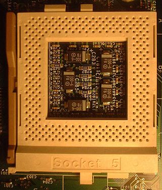
Socket 5 was created for the second generation of Intel P5 Pentium processors operating at speeds from 75 to 133 MHz as well as certain Pentium OverDrive and Pentium MMX processors with core voltage 3.3 V. It superseded the earlier Socket 4. It was released in March 1994. Consisting of 320 pins, this was the first socket to use a staggered pin grid array, or SPGA, which allowed the chip's pins to be spaced closer together than earlier sockets. Socket 5 was replaced by Socket 7 in 1995.
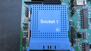
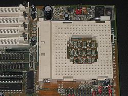
Socket 1, originally called the "OverDrive" socket, was the second of a series of standard CPU sockets created by Intel into which various x86 microprocessors were inserted. It was an upgrade to Intel's first standard 169-pin pin grid array (PGA) socket and the first with an official designation. Socket 1 was intended as a 486 upgrade socket, and added one extra pin to prevent upgrade chips from being inserted incorrectly.

Socket 2 was one of the series of CPU sockets into which various x86 microprocessors were inserted. It was an updated Socket 1 with added support for Pentium OverDrive processors.

Socket 604 is a 604-pin microprocessor socket designed to interface an Intel Xeon processor to the rest of the computer. It provides both an electrical interface as well as physical support. This socket is designed to support a heatsink.
Socket G3, also known as rPGA 946B/947 or FCPGA 946, is a socket for Intel microprocessors that supports Haswell-based mobile CPUs. Compatible SKUs have an 'M' suffix in the model number.
LGA 4677 is a zero insertion force flip-chip land grid array (LGA) CPU socket designed by Intel, compatible with Sapphire Rapids server and workstation processors, which was released in January 2023.