Direct3D is a graphics application programming interface (API) for Microsoft Windows. Part of DirectX, Direct3D is used to render three-dimensional graphics in applications where performance is important, such as games. Direct3D uses hardware acceleration if it is available on the graphics card, allowing for hardware acceleration of the entire 3D rendering pipeline or even only partial acceleration. Direct3D exposes the advanced graphics capabilities of 3D graphics hardware, including Z-buffering, W-buffering, stencil buffering, spatial anti-aliasing, alpha blending, color blending, mipmapping, texture blending, clipping, culling, atmospheric effects, perspective-correct texture mapping, programmable HLSL shaders and effects. Integration with other DirectX technologies enables Direct3D to deliver such features as video mapping, hardware 3D rendering in 2D overlay planes, and even sprites, providing the use of 2D and 3D graphics in interactive media ties.

The High-Level Shader Language or High-Level Shading Language (HLSL) is a proprietary shading language developed by Microsoft for the Direct3D 9 API to augment the shader assembly language, and went on to become the required shading language for the unified shader model of Direct3D 10 and higher.

A graphics processing unit (GPU) is a specialized electronic circuit initially designed to accelerate computer graphics and image processing. After their initial design, GPUs were found to be useful for non-graphic calculations involving embarrassingly parallel problems due to their parallel structure. Other non-graphical uses include the training of neural networks and cryptocurrency mining.
The R420 GPU, developed by ATI Technologies, was the company's basis for its 3rd-generation DirectX 9.0/OpenGL 2.0-capable graphics cards. Used first on the Radeon X800, the R420 was produced on a 0.13 micrometer low-K photolithography process and used GDDR-3 memory. The chip was designed for AGP graphics cards.

In computer graphics, a shader is a computer program that calculates the appropriate levels of light, darkness, and color during the rendering of a 3D scene—a process known as shading. Shaders have evolved to perform a variety of specialized functions in computer graphics special effects and video post-processing, as well as general-purpose computing on graphics processing units.
A shading language is a graphics programming language adapted to programming shader effects. Shading languages usually consist of special data types like "vector", "matrix", "color" and "normal".
AMD FirePro was AMD's brand of graphics cards designed for use in workstations and servers running professional Computer-aided design (CAD), Computer-generated imagery (CGI), Digital content creation (DCC), and High-performance computing/GPGPU applications. The GPU chips on FirePro-branded graphics cards are identical to the ones used on Radeon-branded graphics cards. The end products differentiate substantially by the provided graphics device drivers and through the available professional support for the software. The product line is split into two categories: "W" workstation series focusing on workstation and primarily focusing on graphics and display, and "S" server series focused on virtualization and GPGPU/High-performance computing.
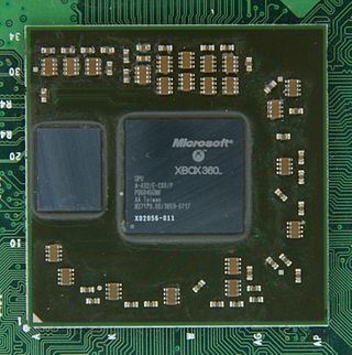
The Xenos is a custom graphics processing unit (GPU) designed by ATI, used in the Xbox 360 video game console developed and produced for Microsoft. Developed under the codename "C1", it is in many ways related to the R520 architecture and therefore very similar to an ATI Radeon X1800 XT series of PC graphics cards as far as features and performance are concerned. However, the Xenos introduced new design ideas that were later adopted in the TeraScale microarchitecture, such as the unified shader architecture. The package contains two separate dies, the GPU and an eDRAM, featuring a total of 337 million transistors.
The R520 is a graphics processing unit (GPU) developed by ATI Technologies and produced by TSMC. It was the first GPU produced using a 90 nm photolithography process.
In computer graphics, a texture mapping unit (TMU) is a component in modern graphics processing units (GPUs). They are able to rotate, resize, and distort a bitmap image to be placed onto an arbitrary plane of a given 3D model as a texture, in a process called texture mapping. In modern graphics cards it is implemented as a discrete stage in a graphics pipeline, whereas when first introduced it was implemented as a separate processor, e.g. as seen on the Voodoo2 graphics card.
Tiled rendering is the process of subdividing a computer graphics image by a regular grid in optical space and rendering each section of the grid, or tile, separately. The advantage to this design is that the amount of memory and bandwidth is reduced compared to immediate mode rendering systems that draw the entire frame at once. This has made tile rendering systems particularly common for low-power handheld device use. Tiled rendering is sometimes known as a "sort middle" architecture, because it performs the sorting of the geometry in the middle of the graphics pipeline instead of near the end.

Tesla is the codename for a GPU microarchitecture developed by Nvidia, and released in 2006, as the successor to Curie microarchitecture. It was named after the pioneering electrical engineer Nikola Tesla. As Nvidia's first microarchitecture to implement unified shaders, it was used with GeForce 8 Series, GeForce 9 Series, GeForce 100 Series, GeForce 200 Series, and GeForce 300 Series of GPUs collectively manufactured in 90 nm, 80 nm, 65 nm, 55 nm, and 40 nm. It was also in the GeForce 405 and in the Quadro FX, Quadro x000, Quadro NVS series, and Nvidia Tesla computing modules.
AMD FireStream was AMD's brand name for their Radeon-based product line targeting stream processing and/or GPGPU in supercomputers. Originally developed by ATI Technologies around the Radeon X1900 XTX in 2006, the product line was previously branded as both ATI FireSTREAM and AMD Stream Processor. The AMD FireStream can also be used as a floating-point co-processor for offloading CPU calculations, which is part of the Torrenza initiative. The FireStream line has been discontinued since 2012, when GPGPU workloads were entirely folded into the AMD FirePro line.

The Northern Islands series is a family of GPUs developed by Advanced Micro Devices (AMD) forming part of its Radeon-brand, based on the 40 nm process. Some models are based on TeraScale 2 (VLIW5), some on the new TeraScale 3 (VLIW4) introduced with them.
Graphics Core Next (GCN) is the codename for a series of microarchitectures and an instruction set architecture that were developed by AMD for its GPUs as the successor to its TeraScale microarchitecture. The first product featuring GCN was launched on January 9, 2012.

The R300 GPU, introduced in August 2002 and developed by ATI Technologies, is its third generation of GPU used in Radeon graphics cards. This GPU features 3D acceleration based upon Direct3D 9.0 and OpenGL 2.0, a major improvement in features and performance compared to the preceding R200 design. R300 was the first fully Direct3D 9-capable consumer graphics chip. The processors also include 2D GUI acceleration, video acceleration, and multiple display outputs.

Pascal is the codename for a GPU microarchitecture developed by Nvidia, as the successor to the Maxwell architecture. The architecture was first introduced in April 2016 with the release of the Tesla P100 (GP100) on April 5, 2016, and is primarily used in the GeForce 10 series, starting with the GeForce GTX 1080 and GTX 1070, which were released on May 17, 2016, and June 10, 2016, respectively. Pascal was manufactured using TSMC's 16 nm FinFET process, and later Samsung's 14 nm FinFET process.
TeraScale is the codename for a family of graphics processing unit microarchitectures developed by ATI Technologies/AMD and their second microarchitecture implementing the unified shader model following Xenos. TeraScale replaced the old fixed-pipeline microarchitectures and competed directly with Nvidia's first unified shader microarchitecture named Tesla.
