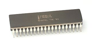
x86 is a family of complex instruction set computer (CISC) instruction set architectures initially developed by Intel based on the Intel 8086 microprocessor and its 8088 variant. The 8086 was introduced in 1978 as a fully 16-bit extension of Intel's 8-bit 8080 microprocessor, with memory segmentation as a solution for addressing more memory than can be covered by a plain 16-bit address. The term "x86" came into being because the names of several successors to Intel's 8086 processor end in "86", including the 80186, 80286, 80386 and 80486 processors. Colloquially, their names were "186", "286", "386" and "486".
In computer architecture, 32-bit computing refers to computer systems with a processor, memory, and other major system components that operate on data in 32-bit units. Compared to smaller bit widths, 32-bit computers can perform large calculations more efficiently and process more data per clock cycle. Typical 32-bit personal computers also have a 32-bit address bus, permitting up to 4 GB of RAM to be accessed, far more than previous generations of system architecture allowed.

VIA Technologies, Inc. is a Taiwanese manufacturer of integrated circuits, mainly motherboard chipsets, CPUs, and memory. It was the world's largest independent manufacturer of motherboard chipsets. As a fabless semiconductor company, VIA conducts research and development of its chipsets in-house, then subcontracts the actual (silicon) manufacturing to third-party merchant foundries such as TSMC.

x86-64 is a 64-bit version of the x86 instruction set, first announced in 1999. It introduced two new modes of operation, 64-bit mode and compatibility mode, along with a new 4-level paging mode.
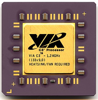
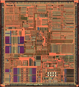
The VIA C3 is a family of x86 central processing units for personal computers designed by Centaur Technology and sold by VIA Technologies. The different CPU cores are built following the design methodology of Centaur Technology.
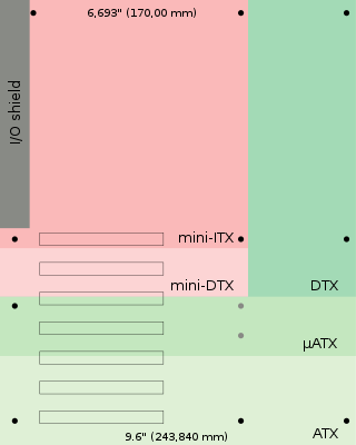
Mini-ITX is a 170 mm × 170 mm motherboard form factor developed by VIA Technologies in 2001. Mini-ITX motherboards have been traditionally used in small-configured computer systems. Originally, Mini-ITX was a niche standard designed for fanless cooling with a low power consumption architecture, which made them useful for home theater PC systems, where fan noise can detract from the cinema experience.
The x86 instruction set refers to the set of instructions that x86-compatible microprocessors support. The instructions are usually part of an executable program, often stored as a computer file and executed on the processor.
The NetBurst microarchitecture, called P68 inside Intel, was the successor to the P6 microarchitecture in the x86 family of central processing units (CPUs) made by Intel. The first CPU to use this architecture was the Willamette-core Pentium 4, released on November 20, 2000 and the first of the Pentium 4 CPUs; all subsequent Pentium 4 and Pentium D variants have also been based on NetBurst. In mid-2001, Intel released the Foster core, which was also based on NetBurst, thus switching the Xeon CPUs to the new architecture as well. Pentium 4-based Celeron CPUs also use the NetBurst architecture.
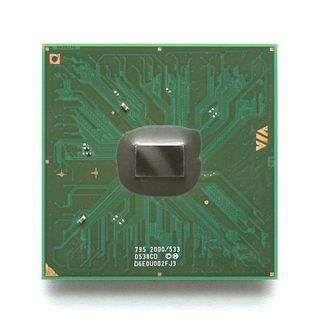
The VIA C7 is an x86 central processing unit designed by Centaur Technology and sold by VIA Technologies.
The P6 microarchitecture is the sixth-generation Intel x86 microarchitecture, implemented by the Pentium Pro microprocessor that was introduced in November 1995. It is frequently referred to as i686. It was planned to be succeeded by the NetBurst microarchitecture used by the Pentium 4 in 2000, but was revived for the Pentium M line of microprocessors. The successor to the Pentium M variant of the P6 microarchitecture is the Core microarchitecture which in turn is also derived from P6.
The Intel Core microarchitecture is a multi-core processor microarchitecture launched by Intel in mid-2006. It is a major evolution over the Yonah, the previous iteration of the P6 microarchitecture series which started in 1995 with Pentium Pro. It also replaced the NetBurst microarchitecture, which suffered from high power consumption and heat intensity due to an inefficient pipeline designed for high clock rate. In early 2004 the new version of NetBurst (Prescott) needed very high power to reach the clocks it needed for competitive performance, making it unsuitable for the shift to dual/multi-core CPUs. On May 7, 2004 Intel confirmed the cancellation of the next NetBurst, Tejas and Jayhawk. Intel had been developing Merom, the 64-bit evolution of the Pentium M, since 2001, and decided to expand it to all market segments, replacing NetBurst in desktop computers and servers. It inherited from Pentium M the choice of a short and efficient pipeline, delivering superior performance despite not reaching the high clocks of NetBurst.

Centaur Technology was an x86 CPU design company started in 1995 and subsequently a wholly owned subsidiary of VIA Technologies. In 2015, the documentary Rise of the Centaur covered the early history of the company. The company was broken up in 2021.

VIA CoreFusion is a line of low power x86 processors manufactured by VIA starting in 2003. The Corefusion integrates the Northbridge, graphics processing unit and a V-Link Interface

In computer design, Pico-ITX is a PC motherboard form factor announced by VIA Technologies in January 2007 and demonstrated later the same year at CeBIT. The formfactor was transferred over to SFF-SIG in 2008. The Pico-ITX form factor specifications call for the board to be 10 × 7.2 cm (3.9 × 2.8 in), which is half the area of Nano-ITX.

The VIA Nano is a 64-bit CPU for personal computers. The VIA Nano was released by VIA Technologies in 2008 after five years of development by its CPU division, Centaur Technology. This new Isaiah 64-bit architecture was designed from scratch, unveiled on 24 January 2008, and launched on 29 May, including low-voltage variants and the Nano brand name. The processor supports a number of VIA-specific x86 extensions designed to boost efficiency in low-power appliances.

Intel Atom is a line of IA-32 and x86-64 instruction set ultra-low-voltage processors by Intel Corporation designed to reduce electric consumption and power dissipation in comparison with ordinary processors of the Intel Core series. Atom is mainly used in netbooks, nettops, embedded applications ranging from health care to advanced robotics, mobile Internet devices (MIDs) and phones. The line was originally designed in 45 nm complementary metal–oxide–semiconductor (CMOS) technology and subsequent models, codenamed Cedar, used a 32 nm process.
Advanced Vector Extensions are SIMD extensions to the x86 instruction set architecture for microprocessors from Intel and Advanced Micro Devices (AMD). They were proposed by Intel in March 2008 and first supported by Intel with the Sandy Bridge processor shipping in Q1 2011 and later by AMD with the Bulldozer processor shipping in Q3 2011. AVX provides new features, new instructions, and a new coding scheme.

Ultra-low-voltage processors are a class of microprocessor that are deliberately underclocked to consume less power, at the expense of performance.
Bonnell is a CPU microarchitecture used by Intel Atom processors which can execute up to two instructions per cycle. Like many other x86 microprocessors, it translates x86 instructions into simpler internal operations prior to execution. The majority of instructions produce one micro-op when translated, with around 4% of instructions used in typical programs producing multiple micro-ops. The number of instructions that produce more than one micro-op is significantly fewer than the P6 and NetBurst microarchitectures. In the Bonnell microarchitecture, internal micro-ops can contain both a memory load and a memory store in connection with an ALU operation, thus being more similar to the x86 level and more powerful than the micro-ops used in previous designs. This enables relatively good performance with only two integer ALUs, and without any instruction reordering, speculative execution or register renaming. A side effect of having no speculative execution is invulnerability against Meltdown and Spectre.


