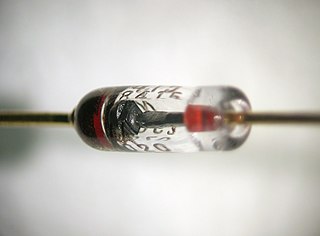
A diode is a two-terminal electronic component that conducts current primarily in one direction ; it has low resistance in one direction, and high resistance in the other.
A semiconductor is a material which has an electrical conductivity value falling between that of a conductor, such as copper, and an insulator, such as glass. Its resistivity falls as its temperature rises; metals behave in the opposite way. Its conducting properties may be altered in useful ways by introducing impurities ("doping") into the crystal structure. When two differently doped regions exist in the same crystal, a semiconductor junction is created. The behavior of charge carriers, which include electrons, ions, and electron holes, at these junctions is the basis of diodes, transistors, and most modern electronics. Some examples of semiconductors are silicon, germanium, gallium arsenide, and elements near the so-called "metalloid staircase" on the periodic table. After silicon, gallium arsenide is the second-most common semiconductor and is used in laser diodes, solar cells, microwave-frequency integrated circuits, and others. Silicon is a critical element for fabricating most electronic circuits.

A transistor is a semiconductor device used to amplify or switch electrical signals and power. The transistor is one of the basic building blocks of modern electronics. It is composed of semiconductor material, usually with at least three terminals for connection to an electronic circuit. A voltage or current applied to one pair of the transistor's terminals controls the current through another pair of terminals. Because the controlled (output) power can be higher than the controlling (input) power, a transistor can amplify a signal. Some transistors are packaged individually, but many more in miniature form are found embedded in integrated circuits.

A semiconductor device is an electronic component that relies on the electronic properties of a semiconductor material for its function. Its conductivity lies between conductors and insulators. Semiconductor devices have replaced vacuum tubes in most applications. They conduct electric current in the solid state, rather than as free electrons across a vacuum or as free electrons and ions through an ionized gas.
A bipolar junction transistor (BJT) is a type of transistor that uses both electrons and electron holes as charge carriers. In contrast, a unipolar transistor, such as a field-effect transistor, uses only one kind of charge carrier. A bipolar transistor allows a small current injected at one of its terminals to control a much larger current flowing between the terminals, making the device capable of amplification or switching.

A p–n junction is a boundary or interface between two types of semiconductor materials, p-type and n-type, inside a single crystal of semiconductor. The "p" (positive) side contains an excess of holes, while the "n" (negative) side contains an excess of electrons in the outer shells of the electrically neutral atoms there. This allows electrical current to pass through the junction only in one direction. The p-n junction is created by doping, for example by ion implantation, diffusion of dopants, or by epitaxy. If two separate pieces of material were used, this would introduce a grain boundary between the semiconductors that would severely inhibit its utility by scattering the electrons and holes.

A high-electron-mobility transistor (HEMT), also known as heterostructure FET (HFET) or modulation-doped FET (MODFET), is a field-effect transistor incorporating a junction between two materials with different band gaps as the channel instead of a doped region. A commonly used material combination is GaAs with AlGaAs, though there is wide variation, dependent on the application of the device. Devices incorporating more indium generally show better high-frequency performance, while in recent years, gallium nitride HEMTs have attracted attention due to their high-power performance. Like other FETs, HEMTs are used in integrated circuits as digital on-off switches. FETs can also be used as amplifiers for large amounts of current using a small voltage as a control signal. Both of these uses are made possible by the FET’s unique current–voltage characteristics. HEMT transistors are able to operate at higher frequencies than ordinary transistors, up to millimeter wave frequencies, and are used in high-frequency products such as cell phones, satellite television receivers, voltage converters, and radar equipment. They are widely used in satellite receivers, in low power amplifiers and in the defense industry.
In semiconductor production, doping is the intentional introduction of impurities into an intrinsic semiconductor for the purpose of modulating its electrical, optical and structural properties. The doped material is referred to as an extrinsic semiconductor.
The heterojunction bipolar transistor (HBT) is a type of bipolar junction transistor (BJT) which uses differing semiconductor materials for the emitter and base regions, creating a heterojunction. The HBT improves on the BJT in that it can handle signals of very high frequencies, up to several hundred GHz. It is commonly used in modern ultrafast circuits, mostly radio frequency (RF) systems, and in applications requiring a high power efficiency, such as RF power amplifiers in cellular phones. The idea of employing a heterojunction is as old as the conventional BJT, dating back to a patent from 1951. Detailed theory of heterojunction bipolar transistor was developed by Herbert Kroemer in 1957.

The point-contact transistor was the first type of transistor to be successfully demonstrated. It was developed by research scientists John Bardeen and Walter Brattain at Bell Laboratories in December 1947. They worked in a group led by physicist William Shockley. The group had been working together on experiments and theories of electric field effects in solid state materials, with the aim of replacing vacuum tubes with a smaller device that consumed less power.

The surface-barrier transistor is a type of transistor developed by Philco in 1953 as an improvement to the alloy-junction transistor and the earlier point-contact transistor. Like the modern Schottky transistor, it offered much higher speed than earlier transistors and used metal–semiconductor junctions, but unlike the schottky transistor, both junctions were metal–semiconductor junctions.
An extrinsic semiconductor is one that has been doped; during manufacture of the semiconductor crystal a trace element or chemical called a doping agent has been incorporated chemically into the crystal, for the purpose of giving it different electrical properties than the pure semiconductor crystal, which is called an intrinsic semiconductor. In an extrinsic semiconductor it is these foreign dopant atoms in the crystal lattice that mainly provide the charge carriers which carry electric current through the crystal. The doping agents used are of two types, resulting in two types of extrinsic semiconductor. An electron donor dopant is an atom which, when incorporated in the crystal, releases a mobile conduction electron into the crystal lattice. An extrinsic semiconductor which has been doped with electron donor atoms is called an n-type semiconductor, because the majority of charge carriers in the crystal are negative electrons. An electron acceptor dopant is an atom which accepts an electron from the lattice, creating a vacancy where an electron should be called a hole which can move through the crystal like a positively charged particle. An extrinsic semiconductor which has been doped with electron acceptor atoms is called a p-type semiconductor, because the majority of charge carriers in the crystal are positive holes.
A tetrode transistor is any transistor having four active terminals.
The drift-field transistor, also called the drift transistor or graded base transistor, is a type of high-speed bipolar junction transistor having a doping-engineered electric field in the base to reduce the charge carrier base transit time.
A diffused junction transistor is a transistor formed by diffusing dopants into a semiconductor substrate. The diffusion process was developed later than the alloy junction and grown junction processes for making bipolar junction transistors (BJTs).

The grown-junction transistor was the first type of bipolar junction transistor made. It was invented by William Shockley at Bell Labs on June 23, 1948, six months after the first bipolar point-contact transistor. The first germanium prototypes were made in 1949. Bell Labs announced Shockley’s grown-junction transistor on July 4, 1951.
A transistor is a semiconductor device with at least three terminals for connection to an electric circuit. In the common case, the third terminal controls the flow of current between the other two terminals. This can be used for amplification, as in the case of a radio receiver, or for rapid switching, as in the case of digital circuits. The transistor replaced the vacuum-tube triode, also called a (thermionic) valve, which was much larger in size and used significantly more power to operate.The first transistor was successfully demonstrated on December 23, 1947, at Bell Laboratories in Murray Hill, New Jersey. Bell Labs was the research arm of American Telephone and Telegraph (AT&T). The three individuals credited with the invention of the transistor were William Shockley, John Bardeen and Walter Brattain. The introduction of the transistor is often considered one of the most important inventions in history.
A definition in semiconductor physics, carrier lifetime is defined as the average time it takes for a minority carrier to recombine. The process through which this is done is typically known as minority carrier recombination.

The 2N107 is an early germanium alloy junction PNP transistor developed by General Electric (GE) in 1955, to become GE's entry into the electronic hobbyist market successfully started with the CK722 transistor. Like the CK722, it enjoyed a long-standing popularity. General Electric decided to designate it with a JEDEC 2N- series identification. This is unusual for a hobby device. Soon after, other manufacturers got involved in the hobby business like Sylvania, Tung-Sol and RCA.

Mohamed M. Atalla was an Egyptian-American engineer, physicist, cryptographer, inventor and entrepreneur. He was a semiconductor pioneer who made important contributions to modern electronics. He is best known for inventing the MOSFET in 1959, which along with Atalla's earlier surface passivation and thermal oxidation processes, revolutionized the electronics industry. He is also known as the founder of the data security company Atalla Corporation, founded in 1972. He received the Stuart Ballantine Medal and was inducted into the National Inventors Hall of Fame for his important contributions to semiconductor technology as well as data security.