Baker clamp

Last updated

Baker clamp is a generic name for a class of electronic circuits that reduce the storage time of a switching bipolar junction transistor (BJT) by applying a nonlinear negative feedback through various kinds of diodes. The reason for slow turn-off times of saturated BJTs is the stored charge in the base. It must be removed before the transistor will turn off since the storage time is a limiting factor of using bipolar transistors and IGBTs in fast switching applications. The diode-based Baker clamps prevent the transistor from saturating and thereby accumulating a lot of stored charge. [1]

Contents

Origin

The standard two-diode Baker clamp circuit, which includes the feedback current I1 that reduces the base current Ib Baker clamp.png
The standard two-diode Baker clamp circuit, which includes the feedback current I1 that reduces the base current Ib
Baker clamp alternative in a Schottky transistor Schottky-Transistor-ersatz.svg
Baker clamp alternative in a Schottky transistor

The Baker clamp is named after Richard H. Baker, who described it in his 1956 technical report "Maximum Efficiency Transistor Switching Circuits." [2] Baker called the technique "back clamping", but the circuit is now called a Baker clamp. Many sources credit Baker's report for the two-diode clamp circuit. [3] [4] [5] Also in 1956, Baker described the circuit in a patent application; the 1961 issued patent, US 3,010,031, [6] claims the use of the clamp in symmetrical flip-flop circuits.

Similar clamp circuits are said to have been known before Baker's report. Kyttälä states, "Although invention of the Baker Clamp circuit is credited to Richard H. Baker (US Patent 3,010,031) it was already common knowledge in 1953 and described in transistor introductory papers that were written by Richard F. Shea." [7] However, Shea's 1953 transistor text does not describe a similar clamp circuit. [8] Shea's 1957 text does describe the clamp circuit and references Baker's technical report. [3]

There are other clamp circuits. A 1959 manual describes a technique called "saturation clamping". [9] In that scheme, there is a saturation clamp supply at about 2 volts connected to the collector with a saturation clamp diode. When the transistor nears saturation, the clamp diode turns on and supplies the extra collector current to keep the transistor from saturating. The saturation clamp supply needs to supply substantial current. [10] In contrast, the Baker clamp reduces the transistor base current rather than supplying more collector current.

Another clamp circuit uses a single diode clamp. [9] It reduces base drive as the transistor nears saturation, but it uses a resistor divider network.

Clamp circuits were also used to speed up cutoff transitions. When the transistor is cutoff, the output is similar to an RC circuit that exponentially decays to its final value. As the circuit gets closer to its final value, there is less current available to charge the capacitor, so the rate of approach lessens. To reach 90 percent of the final value takes about 2.3 time constants. [11] Cutoff clamping reduces the output voltage swing but makes the transition faster. Clamping the collector voltage to 63 percent of the final value allows a factor of two speed increase. [12]

Basic idea

The Baker clamp limits the voltage difference between emitter and collector by diverting base current through the collector. This introduces a nonlinear negative feedback into a common-emitter stage (BJT switch), with the purpose to avoid saturation by decreasing the gain near the saturation point. While the transistor is in active mode and it is far away enough from the saturation point, the negative feedback is turned off and the gain is maximal; when the transistor approaches the saturation point, the negative feedback gradually turns on, and the gain quickly drops. To decrease the gain, the transistor acts as a shunt regulator with regard to its own base–emitter junction: it diverts a part of the base current to ground by connecting a voltage-stable element in parallel to the base–emitter junction.

Implementation

The two-diode Baker clamp circuit is shown in the figure from Baker's patent and in many other publications. [9] The feedback diode (D1) between the collector and the input limits the collector voltage to approximately VBE by diverting the excessive input current through the collector to ground. [13] An additional silicon diode is connected in series with the base terminal to raise the effective input voltage; the clamp diode in the collector–base feedback is sometimes made from germanium to minimize the voltage drop across it. [6] The base diode allows a Si diode clamp to be used with a Si transistor and keeps VCE around a diode drop and much greater than VCE(sat). Unfortunately, it turns off and creates a high-impedance return path when trying to turn the transistor off. Although the base charge has been minimized, it is now more difficult to draw charge out of the base.

A second base diode connected antiparallel to the base diode (D2 in Baker's schematic) will provide a low-impedance return path for removing stored base charge in the transistor. This three-diode circuit is still referred to as a Baker clamp by some sources, [14] while others only call the two-diode circuit a Baker clamp. [15]

A simple alternative to the Baker clamp is a single low-voltage diode from the collector to the base. To work well, the forward drop of the diode must be less than the base–emitter drop, so low-voltage-drop germanium and Schottky diodes can be used with silicon transistors (the forward voltage drop of a Schottky diode is much less than the VBE bias voltage of a silicon transistor and it switches rapidly). An alternative diode clamp circuit connects the diode to a junction of two base-bias resistors. [9] The contemporary solution is to integrate the combination of a Schottky diode and transistor into one Schottky transistor. Some sources also refer to this configuration as a Baker clamp. [16]

Baker clamps are also used in power applications, and the choice of diodes is a significant design issue. [17]

One drawback of the Baker clamp is its increased low voltage-output level (as in a Darlington transistor). In logic circuits, it decreases the noise immunity; in power applications, it increases the dissipated power.

See also

Related Research Articles

Diode Electronic component that only allows current to flow in one direction

A diode is a two-terminal electronic component that conducts current primarily in one direction ; it has low resistance in one direction, and high resistance in the other.

Transistor Solid-state electrically operated switch also used as an amplifier

A transistor is a semiconductor device used to amplify or switch electrical signals and power. The transistor is one of the basic building blocks of modern electronics. It is composed of semiconductor material, usually with at least three terminals for connection to an electronic circuit. A voltage or current applied to one pair of the transistor's terminals controls the current through another pair of terminals. Because the controlled (output) power can be higher than the controlling (input) power, a transistor can amplify a signal. Some transistors are packaged individually, but many more are found embedded in integrated circuits.

Semiconductor device Electronic component that exploits the electronic properties of semiconductor materials

A semiconductor device is an electronic component that relies on the electronic properties of a semiconductor material for its function. Its conductivity lies between conductors and insulators. Semiconductor devices have replaced vacuum tubes in most applications. They conduct electric current in the solid state, rather than as free electrons across a vacuum or as free electrons and ions through an ionized gas.

Transistor–transistor logic (TTL) is a logic family built from bipolar junction transistors. Its name signifies that transistors perform both the logic function and the amplifying function, as opposed to resistor–transistor logic (RTL) or diode–transistor logic (DTL).

Bipolar junction transistor Transistor that uses both electrons and holes as charge carriers

A bipolar junction transistor (BJT) is a type of transistor that uses both electrons and electron holes as charge carriers. In contrast, a unipolar transistor, such as a field-effect transistor, uses only one kind of charge carrier. A bipolar transistor allows a small current injected at one of its terminals to control a much larger current flowing between the terminals, making the device capable of amplification or switching.

In electronics, a multi-transistor configuration called the Darlington configuration is a circuit consisting of two bipolar transistors with the emitter of one transistor connected to the base of the other, such that the current amplified by the first transistor is amplified further by the second one. The collectors of both transistors are connected together. This configuration has a much higher current gain than each transistor taken separately. It acts like and is often packaged as a single transistor. It was invented in 1953 by Sidney Darlington.

Emitter-coupled logic

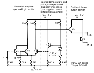
In electronics, emitter-coupled logic (ECL) is a high-speed integrated circuit bipolar transistor logic family. ECL uses an overdriven bipolar junction transistor (BJT) differential amplifier with single-ended input and limited emitter current to avoid the saturated region of operation and its slow turn-off behavior. As the current is steered between two legs of an emitter-coupled pair, ECL is sometimes called current-steering logic (CSL), current-mode logic (CML) or current-switch emitter-follower (CSEF) logic.

Schottky diode Semiconductor diode

The Schottky diode, also known as Schottky barrier diode or hot-carrier diode, is a semiconductor diode formed by the junction of a semiconductor with a metal. It has a low forward voltage drop and a very fast switching action. The cat's-whisker detectors used in the early days of wireless and metal rectifiers used in early power applications can be considered primitive Schottky diodes.

Resistor–transistor logic (RTL) is a class of digital circuits built using resistors as the input network and bipolar junction transistors (BJTs) as switching devices. RTL is the earliest class of transistorized digital logic circuit used; other classes include diode–transistor logic (DTL) and transistor–transistor logic (TTL). RTL circuits were first constructed with discrete components, but in 1961 it became the first digital logic family to be produced as a monolithic integrated circuit. RTL integrated circuits were used in the Apollo Guidance Computer, whose design was begun in 1961 and which first flew in 1966.

Diode–transistor logic (DTL) is a class of digital circuits that is the direct ancestor of transistor–transistor logic. It is called so because the logic gating function is performed by a diode network and the amplifying function is performed by a transistor.

Voltage regulator System designed to maintain a constant voltage

A voltage regulator is a system designed to automatically maintain a constant voltage. A voltage regulator may use a simple feed-forward design or may include negative feedback. It may use an electromechanical mechanism, or electronic components. Depending on the design, it may be used to regulate one or more AC or DC voltages.

Current source Electronic circuit which delivers or absorbs electric current regardless of voltage

A current source is an electronic circuit that delivers or absorbs an electric current which is independent of the voltage across it.

In computer engineering, a logic family is one of two related concepts:

Electronic component Discrete device in an electronic system

An electronic component is any basic discrete device or physical entity in an electronic system used to affect electrons or their associated fields. Electronic components are mostly industrial products, available in a singular form and are not to be confused with electrical elements, which are conceptual abstractions representing idealized electronic components and elements.

An avalanche transistor is a bipolar junction transistor designed for operation in the region of its collector-current/collector-to-emitter voltage characteristics beyond the collector-to-emitter breakdown voltage, called avalanche breakdown region. This region is characterized by avalanche breakdown, which is a phenomenon similar to Townsend discharge for gases, and negative differential resistance. Operation in the avalanche breakdown region is called avalanche-mode operation: it gives avalanche transistors the ability to switch very high currents with less than a nanosecond rise and fall times. Transistors not specifically designed for the purpose can have reasonably consistent avalanche properties; for example 82% of samples of the 15V high-speed switch 2N2369, manufactured over a 12-year period, were capable of generating avalanche breakdown pulses with rise time of 350 ps or less, using a 90V power supply as Jim Williams writes.

Joule thief Voltage booster electronic circuit

A joule thief is a minimalist self-oscillating voltage booster that is small, low-cost, and easy to build, typically used for driving small loads. This circuit is also known by other names such as joule resurrection circuit (JRC), joule ringer, blocking oscillator, vampire torch, or battery vampire. It can use nearly all of the energy in a single-cell electric battery, even far below the voltage where other circuits consider the battery fully discharged ; hence the name, which suggests the notion that the circuit is stealing energy or "joules" from the source – the term is a pun on "jewel thief". The circuit is a variant of the blocking oscillator that forms an unregulated voltage boost converter. The output voltage is increased at the expense of higher current draw on the input, but the integrated (average) current of the output is lowered and brightness of a luminescence decreased.

Schottky transistor

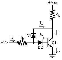
A Schottky transistor is a combination of a transistor and a Schottky diode that prevents the transistor from saturating by diverting the excessive input current. It is also called a Schottky-clamped transistor.

The following outline is provided as an overview of and topical guide to electronics:

James R. Biard American electrical engineer and inventor

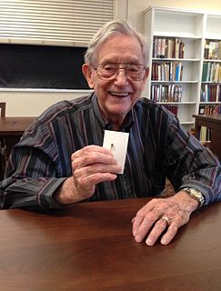
James R. "Bob" Biard is an American electrical engineer and inventor who holds 73 U.S. patents. Some of his more significant patents include the first infrared light-emitting diode (LED), the optical isolator, Schottky clamped logic circuits, silicon Metal Oxide Semiconductor Read Only Memory, a low bulk leakage current avalanche photodetector, and fiber-optic data links. He has been on the staff of Texas A&M University as an Adjunct Professor of Electrical Engineering since 1980.

Field-effect transistor Type of transistor

The field-effect transistor (FET) is a type of transistor that uses an electric field to control the flow of current in a semiconductor. FETs are devices with three terminals: source, gate, and drain. FETs control the flow of current by the application of a voltage to the gate, which in turn alters the conductivity between the drain and source.

References

  1. Simon S. Ang (1995). Power-switching Converters. Marcel Dekker. p. 340. ISBN   978-0-8247-9630-3.
  2. R. H. Baker (1956), "Maximum Efficiency Switching Circuits", MIT Lincoln Laboratory Report TR-110, archived from the original on January 21, 2015
  3. 1 2 Richard F. Shea, ed. (1957). Transistor circuit engineering. Wiley. p. 322.
  4. Ernst Bleuler (1964). Methods of Experimental Physics Vol. 2: Electronic Methods. Academic Press. ISBN   978-0-12-475902-2.
  5. Semiconductor Products Division, Motorola inc.; Roehr, William D.; Thorpe, Darrell (1963). Switching Transistor Handbook. Motorola Semiconductor Products. p. 32.
  6. 1 2 US 3010031,Baker, Richard H.,"Symmetrical Back-Clamped Transistor Switching Circuit",published October 24, 1956,issued November 21, 1961
  7. Kyttälä, Teemu (2008), Solid State Guitar Amplifiers, p. 128, Although invention of the Baker Clamp circuit is credited to Richard H. Baker (US Patent 3,010,031) it was already common knowledge in 1953 and described in transistor introductory papers that were written by Richard F. Shea.
  8. Shea, Richard F., ed. (1953), Principles of Transistor Circuits, New York: Wiley; also published by Chapman & Hall, London
  9. 1 2 3 4 Department of the Army (1963) [1959], Basic Theory and Application of Transistors; Technical Manual 11-690, Dover, pp. 195–199
  10. The transistor collector current will be IC = βIB; whatever does not come from the load will come from the saturation clamp supply.
  11. ln(10.9)=2.302585
  12. ln(10.63)=0.99425
  13. Neil Chadderton and Dino Rosaldi (May 1996). "High Frequency DC-DC Conversion using High Current Bipolar Transistors: 400kHz Operation with Optimised Geometry Devices" (PDF). Zetex. Archived from the original (PDF) on 2009-12-22.
  14. Roehr, William D., ed. (2001), Rectifier Applications Manual: Reference Manual and Design Guide (PDF) (revision 2 ed.), ON Semiconductor, archived from the original (PDF) on 2009-04-07, retrieved 2009-04-20 Pages 175–176 describe a 3-diode "Baker clamp".
  15. Harry E. Thomas (1968). Handbook of transistors, semiconductors, instruments, and microelectronics. Prentice-Hall. p. 228.
  16. Paul Horowitz and Winfield Hill (1989), The Art of Electronics (Second ed.), Cambridge University Press, p. 908, ISBN   978-0-521-37095-0
  17. Pressman, Abraham I. (1998), Switching Power Supply Design (2nd ed.), McGraw-Hill, pp. 328–330, ISBN   0-07-052236-7