
The router is a power tool with a flat base and a rotating blade extending past the base. The spindle may be driven by an electric motor or by a pneumatic motor. It routs an area in hard material, such as wood or plastic. Routers are used most often in woodworking, especially cabinetry. They may be handheld or affixed to router tables. Some woodworkers consider the router one of the most versatile power tools.

A printed circuit board (PCB), also called printed wiring board (PWB), is a medium used to connect or "wire" components to one another in a circuit. It takes the form of a laminated sandwich structure of conductive and insulating layers: each of the conductive layers is designed with a pattern of traces, planes and other features etched from one or more sheet layers of copper laminated onto and/or between sheet layers of a non-conductive substrate. Electrical components may be fixed to conductive pads on the outer layers in the shape designed to accept the component's terminals, generally by means of soldering, to both electrically connect and mechanically fasten them to it. Another manufacturing process adds vias, plated-through holes that allow interconnections between layers.

A ball grid array (BGA) is a type of surface-mount packaging used for integrated circuits. BGA packages are used to permanently mount devices such as microprocessors. A BGA can provide more interconnection pins than can be put on a dual in-line or flat package. The whole bottom surface of the device can be used, instead of just the perimeter. The traces connecting the package's leads to the wires or balls which connect the die to package are also on average shorter than with a perimeter-only type, leading to better performance at high speeds.

Flexible electronics, also known as flex circuits, is a technology for assembling electronic circuits by mounting electronic devices on flexible plastic substrates, such as polyimide, PEEK or transparent conductive polyester film. Additionally, flex circuits can be screen printed silver circuits on polyester. Flexible electronic assemblies may be manufactured using identical components used for rigid printed circuit boards, allowing the board to conform to a desired shape, or to flex during its use.

Flip chip, also known as controlled collapse chip connection or its abbreviation, C4, is a method for interconnecting dies such as semiconductor devices, IC chips, integrated passive devices and microelectromechanical systems (MEMS), to external circuitry with solder bumps that have been deposited onto the chip pads. The technique was developed by General Electric's Light Military Electronics Department, Utica, New York. The solder bumps are deposited on the chip pads on the top side of the wafer during the final wafer processing step. In order to mount the chip to external circuitry, it is flipped over so that its top side faces down, and aligned so that its pads align with matching pads on the external circuit, and then the solder is reflowed to complete the interconnect. This is in contrast to wire bonding, in which the chip is mounted upright and fine wires are welded onto the chip pads and lead frame contacts to interconnect the chip pads to external circuitry.

Drill bits are cutting tools used in a drill to remove material to create holes, almost always of circular cross-section. Drill bits come in many sizes and shapes and can create different kinds of holes in many different materials. In order to create holes drill bits are usually attached to a drill, which powers them to cut through the workpiece, typically by rotation. The drill will grasp the upper end of a bit called the shank in the chuck.

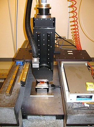
Printed circuit board milling is the milling process used for removing areas of copper from a sheet of printed circuit board (PCB) material to recreate the pads, signal traces and structures according to patterns from a digital circuit board plan known as a layout file. Similar to the more common and well known chemical PCB etch process, the PCB milling process is subtractive: material is removed to create the electrical isolation and ground planes required. However, unlike the chemical etch process, PCB milling is typically a non-chemical process and as such it can be completed in a typical office or lab environment without exposure to hazardous chemicals. High quality circuit boards can be produced using either process. In the case of PCB milling, the quality of a circuit board is chiefly determined by the system's true, or weighted, milling accuracy and control as well as the condition of the milling bits and their respective feed/rotational speeds. By contrast, in the chemical etch process, the quality of a circuit board depends on the accuracy and/or quality of the mask used to protect the copper from the chemicals and the state of the etching chemicals.

Metal fabrication is the creation of metal structures by cutting, bending and assembling processes. It is a value-added process involving the creation of machines, parts, and structures from various raw materials.

Vacuum forming is a simplified version of thermoforming, where a sheet of plastic is heated to a forming temperature, stretched onto a single-surface mould, and forced against the mould by a vacuum. This process can be used to form plastic into permanent objects such as turnpike signs and protective covers. Normally draft angles are present in the design of the mould to ease removal of the formed plastic part from the mould.
Diamond turning is turning using a cutting tool with a diamond tip. It is a process of mechanical machining of precision elements using lathes or derivative machine tools equipped with natural or synthetic diamond-tipped tool bits. The term single-point diamond turning (SPDT) is sometimes applied, although as with other lathe work, the "single-point" label is sometimes only nominal. The process of diamond turning is widely used to manufacture high-quality aspheric optical elements from crystals, metals, acrylic, and other materials. Plastic optics are frequently molded using diamond turned mold inserts. Optical elements produced by the means of diamond turning are used in optical assemblies in telescopes, video projectors, missile guidance systems, lasers, scientific research instruments, and numerous other systems and devices. Most SPDT today is done with computer numerical control (CNC) machine tools. Diamonds also serve in other machining processes, such as milling, grinding, and honing. Diamond turned surfaces have a high specular brightness and require no additional polishing or buffing, unlike other conventionally machined surfaces.

Sheet metal is metal formed into thin, flat pieces, usually by an industrial process.
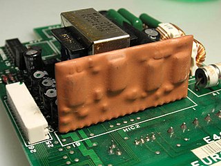
A hybrid integrated circuit (HIC), hybrid microcircuit, hybrid circuit or simply hybrid is a miniaturized electronic circuit constructed of individual devices, such as semiconductor devices and passive components, bonded to a substrate or printed circuit board (PCB). A PCB having components on a Printed Wiring Board (PWB) is not considered a true hybrid circuit according to the definition of MIL-PRF-38534.
Conformal coating is a protective, breathable coating of thin polymeric film applied to printed circuit boards (PCBs). Conformal coatings are typically applied at 25–250 μm to the electronic circuitry and provide protection against moisture and other harsher conditions.
Die singulation, also called wafer dicing, is the process in semiconductor device fabrication by which dies are separated from a finished wafer of semiconductor. Die singulation comes after the photolithography process. It can involve scribing and breaking, mechanical sawing or laser cutting. All methods are typically automated to ensure precision and accuracy. Following the dicing process the individual silicon chips may be encapsulated into chip carriers which are then suitable for use in building electronic devices such as computers, etc.

Sputter deposition is a physical vapor deposition (PVD) method of thin film deposition by the phenomenon of sputtering. This involves ejecting material from a "target" that is a source onto a "substrate" such as a silicon wafer. Resputtering is re-emission of the deposited material during the deposition process by ion or atom bombardment. Sputtered atoms ejected from the target have a wide energy distribution, typically up to tens of eV. The sputtered ions can ballistically fly from the target in straight lines and impact energetically on the substrates or vacuum chamber. Alternatively, at higher gas pressures, the ions collide with the gas atoms that act as a moderator and move diffusively, reaching the substrates or vacuum chamber wall and condensing after undergoing a random walk. The entire range from high-energy ballistic impact to low-energy thermalized motion is accessible by changing the background gas pressure. The sputtering gas is often an inert gas such as argon. For efficient momentum transfer, the atomic weight of the sputtering gas should be close to the atomic weight of the target, so for sputtering light elements neon is preferable, while for heavy elements krypton or xenon are used. Reactive gases can also be used to sputter compounds. The compound can be formed on the target surface, in-flight or on the substrate depending on the process parameters. The availability of many parameters that control sputter deposition make it a complex process, but also allow experts a large degree of control over the growth and microstructure of the film.

Photochemical machining (PCM), also known as photochemical milling or photo etching, is a chemical milling process used to fabricate sheet metal components using a photoresist and etchants to corrosively machine away selected areas. This process emerged in the 1960s as an offshoot of the printed circuit board industry. Photo etching can produce highly complex parts with very fine detail accurately and economically.

Thick-film technology is used to produce electronic devices/modules such as surface mount devices modules, hybrid integrated circuits, heating elements, integrated passive devices and sensors. Main manufacturing technique is screen printing (stenciling), which in addition to use in manufacturing electronic devices can also be used for various graphic reproduction targets. It became one of the key manufacturing/miniaturisation techniques of electronic devices/modules during 1950s. Typical film thickness – manufactured with thick film manufacturing processes for electronic devices – is 0.0001 to 0.1 mm.
Pad cratering is a mechanically induced fracture in the resin between copper foil and outermost layer of fiberglass of a printed circuit board (PCB). It may be within the resin or at the resin to fiberglass interface.
Digital image correlation analyses have applications in material property characterization, displacement measurement, and strain mapping. As such, DIC is becoming an increasingly popular tool when evaluating the thermo-mechanical behavior of electronic components and systems.
In electronics, a cross section, cross-section, or microsection, is a prepared electronics sample that allows analysis at a plane that cuts through the sample. It is a destructive technique requiring that a portion of the sample be cut or ground away to expose the internal plane for analysis. They are commonly prepared for research, manufacturing quality assurance, supplier conformity, and failure analysis. Printed wiring boards (PWBs) and electronic components and their solder joints are common cross sectioned samples. The features of interest to be analyzed in cross section can be nanometer-scale metal and dielectric layers in semiconductors up to macroscopic features such as the amount of solder that has filled into a large, 0.125in (3.18mm) diameter plated through hole.
