Related Research Articles

Semiconductor device fabrication is the process used to manufacture semiconductor devices, typically integrated circuits (ICs) such as computer processors, microcontrollers, and memory chips that are present in everyday electronic devices. It is a multiple-step photolithographic and physio-chemical process during which electronic circuits are gradually created on a wafer, typically made of pure single-crystal semiconducting material. Silicon is almost always used, but various compound semiconductors are used for specialized applications.

Electronic test equipment is used to create signals and capture responses from electronic devices under test (DUTs). In this way, the proper operation of the DUT can be proven or faults in the device can be traced. Use of electronic test equipment is essential to any serious work on electronics systems.

Flip chip, also known as controlled collapse chip connection or its abbreviation, C4, is a method for interconnecting dies such as semiconductor devices, IC chips, integrated passive devices and microelectromechanical systems (MEMS), to external circuitry with solder bumps that have been deposited onto the chip pads. The technique was developed by General Electric's Light Military Electronics Department, Utica, New York. The solder bumps are deposited on the chip pads on the top side of the wafer during the final wafer processing step. In order to mount the chip to external circuitry, it is flipped over so that its top side faces down, and aligned so that its pads align with matching pads on the external circuit, and then the solder is reflowed to complete the interconnect. This is in contrast to wire bonding, in which the chip is mounted upright and fine wires are welded onto the chip pads and lead frame contacts to interconnect the chip pads to external circuitry.
Wafer testing is a step performed during semiconductor device fabrication after the back end of line (BEOL) process is finished. During this step, performed before a wafer is sent to die preparation, all individual integrated circuits that are present on the wafer are tested for functional defects by applying special test patterns to them. The wafer testing is performed by a piece of test equipment called a wafer prober. The process of wafer testing can be referred to in several ways: Wafer Final Test (WFT), Electronic Die Sort (EDS) and Circuit Probe (CP) are probably the most common.
Teradyne, Inc., is an American automatic test equipment (ATE) designer and manufacturer based in North Reading, Massachusetts. Teradyne's high-profile customers include Samsung, Qualcomm, Intel, Analog Devices, Texas Instruments and IBM.

Automatic test equipment or automated test equipment (ATE) is any apparatus that performs tests on a device, known as the device under test (DUT), equipment under test (EUT) or unit under test (UUT), using automation to quickly perform measurements and evaluate the test results. An ATE can be a simple computer-controlled digital multimeter, or a complicated system containing dozens of complex test instruments capable of automatically testing and diagnosing faults in sophisticated electronic packaged parts or on wafer testing, including system on chips and integrated circuits.
Wafer-scale integration (WSI) is a system of building very-large integrated circuit networks from an entire silicon wafer to produce a single "super-chip". Combining large size and reduced packaging, WSI was expected to lead to dramatically reduced costs for some systems, notably massively parallel supercomputers but is now being employed for deep learning. The name is taken from the term very-large-scale integration, the state of the art when WSI was being developed.
Design for testing or design for testability (DFT) consists of IC design techniques that add testability features to a hardware product design. The added features make it easier to develop and apply manufacturing tests to the designed hardware. The purpose of manufacturing tests is to validate that the product hardware contains no manufacturing defects that could adversely affect the product's correct functioning.
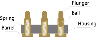
A bed of nails tester is a traditional electronic test fixture used for in-circuit testing. It has numerous pins inserted into holes in an epoxy phenolic glass cloth laminated sheet (G-10) which are aligned using tooling pins to make contact with test points on a printed circuit board and are also connected to a measuring unit by wires. Named by analogy with a real-world bed of nails, these devices contain an array of small, spring-loaded pogo pins; each pogo pin makes contact with one node in the circuitry of the DUT. By pressing the DUT down against the bed of nails, reliable contact can be quickly and simultaneously made with hundreds or even thousands of individual test points within the circuitry of the DUT. The hold-down force may be provided manually or by means of a vacuum or a mechanical presser, thus pulling the DUT downwards onto the nails.

Integrated circuit design, or IC design, is a sub-field of electronics engineering, encompassing the particular logic and circuit design techniques required to design integrated circuits, or ICs. ICs consist of miniaturized electronic components built into an electrical network on a monolithic semiconductor substrate by photolithography.
A test engineer is a professional who determines how to create a process that would best test a particular product in manufacturing and related disciplines, in order to assure that the product meets applicable specifications. Test engineers are also responsible for determining the best way a test can be performed in order to achieve adequate test coverage. Often test engineers also serve as a liaison between manufacturing, design engineering, sales engineering and marketing communities as well.
Electronic packaging is the design and production of enclosures for electronic devices ranging from individual semiconductor devices up to complete systems such as a mainframe computer. Packaging of an electronic system must consider protection from mechanical damage, cooling, radio frequency noise emission and electrostatic discharge. Product safety standards may dictate particular features of a consumer product, for example, external case temperature or grounding of exposed metal parts. Prototypes and industrial equipment made in small quantities may use standardized commercially available enclosures such as card cages or prefabricated boxes. Mass-market consumer devices may have highly specialized packaging to increase consumer appeal. Electronic packaging is a major discipline within the field of mechanical engineering.

A probe card is used in automated integrated circuit testing. It is an interface between an electronic test system and a semiconductor wafer.
Package on a package (PoP) is an integrated circuit packaging method to vertically combine discrete logic and memory ball grid array (BGA) packages. Two or more packages are installed atop each other, i.e. stacked, with a standard interface to route signals between them. This allows higher component density in devices, such as mobile phones, personal digital assistants (PDA), and digital cameras, at the cost of slightly higher height requirements. Stacks with more than 2 packages are uncommon, due to heat dissipation considerations.
Non contact wafer testing is a normal step in semiconductor device fabrication, used to detect defects in integrated circuits (IC) before they are assembled during the IC packaging step.
Reliability of a semiconductor device is the ability of the device to perform its intended function during the life of the device in the field.
Memory testers are specialized test equipment used to test and verify memory modules.

Wafer-level packaging (WLP) is a process where packaging components are attached to an integrated circuit (IC) before the wafer – on which the IC is fabricated – is diced. In WSP, the top and bottom layers of the packaging and the solder bumps are attached to the integrated circuits while they are still in the wafer. This process differs from a conventional process, in which the wafer is sliced into individual circuits (dice) before the packaging components are attached.
Circuit Check is an American company with about 225 employees and seven direct operations in six countries. Headquartered in Maple Grove, Minnesota, it is one of the largest manufacturers of electronic and mechanical test fixtures in North America, . The company also manufactures Automatic Test Equipment for end-of-line manufacturing test. The company uses either a Microsoft Excel-driven "CCITest" software platform, or the National Instruments LabVIEW software platform. They have a variety of clients in different industries which include: Automotive, Military & Aerospace, Medical, Industrial, and Computer Networking.

An audio analyzer is a test and measurement instrument used to objectively quantify the audio performance of electronic and electro-acoustical devices. Audio quality metrics cover a wide variety of parameters, including level, gain, noise, harmonic and intermodulation distortion, frequency response, relative phase of signals, interchannel crosstalk, and more. In addition, many manufacturers have requirements for behavior and connectivity of audio devices that require specific tests and confirmations.
References
- ↑ "Performance Test Terminology for EtherNet/IP Devices" (PDF). Archived from the original (PDF) on 2016-09-14. Retrieved 2022-01-24.
- ↑ "What is a Device Under Test (DUT)? - Definition from Techopedia". Techopedia.com. Retrieved 2019-08-30.
| | This technology-related article is a stub. You can help Wikipedia by expanding it. |