
A transistor is a semiconductor device used to amplify or switch electronic signals and electrical power. It is composed of semiconductor material usually with at least three terminals for connection to an external circuit. A voltage or current applied to one pair of the transistor's terminals controls the current through another pair of terminals. Because the controlled (output) power can be higher than the controlling (input) power, a transistor can amplify a signal. Today, some transistors are packaged individually, but many more are found embedded in integrated circuits.
A semiconductor device is an electronic component that relies on the electronic properties of a semiconductor material for its function. Semiconductor devices have replaced vacuum tubes in most applications. They use electrical conduction in the solid state rather than the gaseous state or thermionic emission in a vacuum.

The metal–oxide–semiconductor field-effect transistor, also known as the metal–oxide–silicon transistor, is a type of insulated-gate field-effect transistor that is fabricated by the controlled oxidation of a semiconductor, typically silicon. The voltage of the covered gate determines the electrical conductivity of the device; this ability to change conductivity with the amount of applied voltage can be used for amplifying or switching electronic signals.
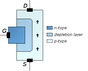
The junction gate field-effect transistor (JFET) is one of the simplest types of field-effect transistor. JFETs are three-terminal semiconductor devices that can be used as electronically-controlled switches, amplifiers, or voltage-controlled resistors.
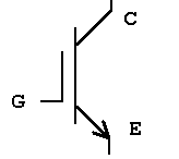
A bipolar junction transistor (BJT) is a type of transistor that uses both electrons and holes as charge carriers. Unipolar transistors, such as field-effect transistors, use only one kind of charge carrier. A bipolar transistor allows a small current injected at one of its terminals to control a much larger current flowing between two other terminals, making the device capable of amplification or switching.
A unijunction transistor (UJT) is a three-lead electronic semiconductor device with only one junction that acts exclusively as an electrically controlled switch.
An insulated-gate bipolar transistor (IGBT) is a three-terminal power semiconductor device primarily used as an electronic switch which, as it was developed, came to combine high efficiency and fast switching. It consists of four alternating layers (P-N-P-N) that are controlled by a metal–oxide–semiconductor (MOS) gate structure without regenerative action. Although the structure of the IGBT is topologically the same as a thyristor with a 'MOS' gate, the thyristor action is completely suppressed and only the transistor action is permitted in the entire device operation range. It is used in switching power supplies in high-power applications: variable-frequency drives (VFDs), electric cars, trains, variable speed refrigerators, lamp ballasts, arc-welding machines, and air conditioners.
A power semiconductor device is a semiconductor device used as a switch or rectifier in power electronics. Such a device is also called a power device or, when used in an integrated circuit, a power IC.
A MESFET is a field-effect transistor semiconductor device similar to a JFET with a Schottky (metal–semiconductor) junction instead of a p–n junction for a gate.
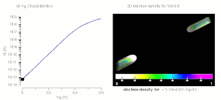
The threshold voltage, commonly abbreviated as Vth, of a field-effect transistor (FET) is the minimum gate-to-source voltage VGS (th) that is needed to create a conducting path between the source and drain terminals. It is an important scaling factor to maintain power efficiency.

An electronic component is any basic discrete device or physical entity in an electronic system used to affect electrons or their associated fields. Electronic components are mostly industrial products, available in a singular form and are not to be confused with electrical elements, which are conceptual abstractions representing idealized electronic components.

A power MOSFET is a specific type of metal–oxide–semiconductor field-effect transistor (MOSFET) designed to handle significant power levels. Compared to the other power semiconductor devices, such as an insulated-gate bipolar transistor (IGBT) or a thyristor, its main advantages are high switching speed and good efficiency at low voltages. It shares with the IGBT an isolated gate that makes it easy to drive. They can be subject to low gain, sometimes to a degree that the gate voltage needs to be higher than the voltage under control.

An electronic symbol is a pictogram used to represent various electrical and electronic devices or functions, such as wires, batteries, resistors, and transistors, in a schematic diagram of an electrical or electronic circuit. These symbols are largely standardized internationally today, but may vary from country to country, or engineering discipline, based on traditional conventions.

A VMOS transistor is a type of MOSFET. VMOS is also used for describing the V-groove shape vertically cut into the substrate material. VMOS is an acronym for "vertical metal oxide semiconductor", or "V-groove MOS".
An H-bridge is an electronic circuit that switches the polarity of a voltage applied to a load. These circuits are often used in robotics and other applications to allow DC motors to run forwards or backwards.
In electronics, cut-off is a state of negligible conduction that is a property of several types of electronic components when a control parameter, is lowered or increased past a value. The transition from normal conduction to cut-off can be more or less sharp, depending on the type of device considered, and also the speed of this transition varies considerably.
An extrinsic semiconductor is one that has been doped; during manufacture of the semiconductor crystal a trace element or chemical called a doping agent has been incorporated chemically into the crystal, for the purpose of giving it different electrical properties than the pure semiconductor crystal, which is called an intrinsic semiconductor. In an extrinsic semiconductor it is these foreign dopant atoms in the crystal lattice that mainly provide the charge carriers which carry electric current through the crystal. The doping agents used are of two types, resulting in two types of extrinsic semiconductor. An electron donor dopant is an atom which, when incorporated in the crystal, releases a mobile conduction electron into the crystal lattice. An extrinsic semiconductor which has been doped with electron donor atoms is called an n-type semiconductor, because the majority of charge carriers in the crystal are negative electrons. An electron acceptor dopant is an atom which accepts an electron from the lattice, creating a vacancy where an electron should be called a hole which can move through the crystal like a positively charged particle. An extrinsic semiconductor which has been doped with electron acceptor atoms is called a p-type semiconductor, because the majority of charge carriers in the crystal are positive holes.

In field-effect transistors (FETS), depletion mode and enhancement mode are two major transistor types, corresponding to whether the transistor is in an ON state or an OFF state at zero gate-source voltage.

The field-effect transistor (FET) is a type of transistor which uses an electric field to control the flow of current. FETs are devices with three terminals: source, gate, and drain. FETs control the flow of current by the application of a voltage to the gate, which in turn alters the conductivity between the drain and source.
A transmission gate (TG) is an analog gate similar to a relay that can conduct in both directions or block by a control signal with almost any voltage potential. It is a CMOS-based switch, in which PMOS passes a strong 1 but poor 0, and NMOS passes strong 0 but poor 1. Both PMOS and NMOS work simultaneously.
