Eutectic bonding

Last updated
Ultrasonic image of a blank Au-Si eutectic bonded wafer B-e-ultrasonicimageofblankeutecticwafer.png
Ultrasonic image of a blank Au-Si eutectic bonded wafer
Ultrasonic image of a patterned Au-Si eutectic bonded wafer B-e-ultrasonicimage.png
Ultrasonic image of a patterned Au-Si eutectic bonded wafer

Eutectic bonding, also referred to as eutectic soldering, describes a wafer bonding technique with an intermediate metal layer that can produce a eutectic system. Those eutectic metals are alloys that transform directly from solid to liquid state, or vice versa from liquid to solid state, at a specific composition and temperature without passing a two-phase equilibrium, i.e. liquid and solid state. The fact that the eutectic temperature can be much lower than the melting temperature of the two or more pure elements can be important in eutectic bonding.[ citation needed ]

Contents

Eutectic alloys are deposited by sputtering, dual source evaporation or electroplating. They can also be formed by diffusion reactions of pure materials and subsequently melting of the eutectic composition. [2]

Eutectic bonding to transfer epitaxial materials such as GaAs-AlGaAs onto Si substrates with high yields for the general purpose of optoelectronics integration with Si electronics as well as to overcome fundamental issues such as lattice mismatch in hetero-epitaxy, was developed and reported by Venkatasubramanian et al. in 1992, and the performance of eutectic-bonded GaAs-AlGaAs materials for solar cells was further validated and reported by the same group in 1994. [3] [4]

Eutectic bonding is able to produce hermetically sealed packages and electrical interconnection within a single process (compare ultrasonic images)[ further explanation needed ]. This procedure is conducted at low temperatures, which results in low resultant stress induced in final assembly, high bonding strength, large fabrication yield and a good reliability. These attributes are dependent on the coefficient of thermal expansion between the substrates. [1]

The most important parameters for eutectic bonding are:

Overview

Eutectic bonding is based on the ability of silicon (Si) to alloy with numerous metals and form a eutectic system. The most established eutectic formations are Si with gold (Au) or with aluminium (Al). [5] This bonding procedure is most commonly used for Si or glass wafers that are coated with an Au/Al film and partly with adhesive layer (compare with following image).

Bonding of Si wafer to (l) glass or (r) silicon wafer coated with Au or Al layer. B-e-coatedsurface.png
Bonding of Si wafer to (l) glass or (r) silicon wafer coated with Au or Al layer.

The Si-Au couple has the advantages of an exceptionally low eutectic temperature, an already widespread use in die bonding and the compatibility with Al interconnects. [6] Additionally, often used eutectic alloys for wafer bonding in semiconductor fabrication are shown in the table. Choosing the correct alloy is determined by the processing temperature and compatibility of the materials used. [7]

Commonly used eutectic alloys
Eutectic alloyEutectic compositionEutectic temperature
Au-In0.6 / 99.4 wt-%156 °C
Cu-Sn5 / 95 wt-%231 °C
Au-Sn [8] 80 / 20 wt-%280 °C
Au-Ge72 / 28 wt-%361 °C
Au-Si97.15 / 2.85 wt-%370 °C
Al-Ge [9] 49 / 51 wt-%419 °C
Al-Si87.5 / 12.5 wt-%580 °C
Si-Au phase diagram. B-e-phasediagram.png
Si-Au phase diagram.

Further, the bonding has less restrictions, concerning substrate roughness and planarity than direct bonding. Compared to anodic bonding, no high voltages are required that can be detrimental to electrostatic MEMS. Additionally, the eutectic bonding procedure promotes a better out-gassing and hermeticity than bonding with organic intermediate layers. [10] Compared to glass frit bonding, the advantage sticks out that the reduction of seal ring geometries, an increase of the hermeticity levels and a shrinking of device size is possible. The geometry of eutectic seals is characterized by a thickness of 1 - 5 μm and a wideness of > 50 μm. The use of eutectic alloy brings the advantage of providing electrical conduction and interfacing with redistribution layers.

The temperature of the eutectic bonding procedure is dependent on the used material. The bonding happens at a specific weight-% and temperature, e.g. 370 °C at 2.85 wt-% Si for Au intermediate layer (compare to phase diagram). [5]

The procedure of eutectic bonding is divided into following steps: [11]

  1. Substrate processing
  2. Conditioning prior to bonding (e.g. oxide removal)
  3. Bonding process (Temperature, Mechanical Pressure for a few minutes)
  4. Cooling process

Procedural steps

Pre-treatment

The surface preparation is the most important step to accomplish a successful eutectic bonding. Prior to preparation the oxide on the silicon surface acts as a diffusion barrier; the eutectic metal bond must be formed against clean silicon. [6] [12]

To remove existing native oxide layers wet chemical etching (HF clean), dry chemical etching or chemical vapor deposition (CVD) with different types of crystals can be used. Also some applications require a surface pre-treatment using dry oxide removal processes, e.g. H2 plasma and CF4 plasma. [1]

An additional method for the removal of unwanted surface films, i.e. oxide, is applying ultrasound during the attachment process. [13] As soon the tool is lowered[ where? ] a relative vibration between the wafer and the substrate is applied. Commonly, industrial bonders use ultrasonic with 60KHz vibration frequencies and 100 μm vibration amplitude. [14] A successful oxide removal results in a solid, hermetically tight connection. [5]

Scheme of typical wafer composition including an optional layer of Ni/Pt. B-e-wafercomposition.png
Scheme of typical wafer composition including an optional layer of Ni/Pt.

A Second method to ensure the eutectic metal adheres on the Si wafer is by using an adhesion layer. This thin intermediate metal layer adheres well to the oxide and the eutectic metal. Well suitable metals for an Au-Si compound are titanium (Ti) and chromium (Cr) resulting in, e.g. Si-SiO2-Ti-Au or Si-SiO2-Cr-Au. The adhesion layer is used to break up the oxide by diffusion of silicon into the used material. A typical wafer is composed of a silicon wafer with oxide, 30 - 200 nm Ti or Cr layer and Au layer of > 500 nm thickness.[ citation needed ]

In the wafer fabrication a nickel (Ni) or a platinum (Pt) layer is added between the gold and the substrate wafer as diffusion barrier. [10] The diffusion barrier avoids interaction between Au and Ti/Cr and requires higher temperatures to form a reliable and uniform bond. Further, the very limited solubility of silicon in titanium and chromium can prevent the developing of Au-Si eutectic composition based on the diffusion of silicon through titanium into gold.[ clarification needed ] [6]

The eutectic materials and optional adhesion layers are usually bonded by deposition as an alloy in one layer by dual component electroplating, dual-source evaporation (physical vapor deposition), or composite alloy sputtering. [12]

The removal of contamination, on the for silicon most established Au layer, is usually realized with water flushing and wafer heating.[ incomprehensible ] [1]

Bonding process

The contacting of the substrates is applied directly after the pre-treatment of the surfaces to avoid oxide regeneration. The bonding procedure for oxidizing metals (not Au) generally takes place in a reduced atmosphere of 4% hydrogen and an inert carrier gas flow, e.g. nitrogen. The requirements for the bonding equipment lies in the thermal and pressure uniformity across the wafer. This enables uniformly compressed seal lines. [2]

The substrate is aligned and fixed on a heated stage and the silicon wafer in a heated tool. The substrates inserted in the bonding chamber are contacted maintaining the alignment. As soon the layers are in atomic contact the reaction between those starts. To support the reaction mechanical pressure is applied and heating above the eutectic temperature is carried out. [1]

The diffusivity and solubility of gold into silicon substrate increases with rising bonding temperatures. A higher temperature than the eutectic temperature is usually preferred for the bonding procedure. This may result in the formation of a thicker Au-Si alloy layer and further a stronger eutectic bond. [15]

The diffusion starts as soon as the layers are in atomic contact at elevated temperatures. [1] The contacted surface layer containing the eutectic composites melts, forming a liquid phase alloy, accelerating further mixing processes and diffusion until the saturation composition is reached. [16] [17]

Other common eutectic bonding alloys commonly used for wafer bonding include Au-Sn, Al-Ge, Au-Ge, Au-In and Cu-Sn. [9]

The chosen bonding temperature usually is some degrees higher than the eutectic temperature so the melt becomes less viscous and readily flows due to higher roughness to surface areas that are not in atomic contact. [12] To prevent the melt pressed outside the bonding interface the optimization of the bonding parameter control is necessary, e.g. low force on the wafers. Otherwise, it may lead to short circuits or device malfunctions of the used components (electrical and mechanical). [1] The heating of the wafers leads to a change in the surface texture due to formation of fine silicon micro structures on top of the gold surface. [17]

Cooling process

Cross-section SEM image of the bonding interface between Si and Au with 80.3 Si atom percentage. B-e-crosssectionsemofbondinginterface.png
Cross-section SEM image of the bonding interface between Si and Au with 80.3 Si atom percentage.

The material mix is solidified when the temperature decreases below eutectic point or the concentration ratio changes (for Si-Au: T < 370 °C). [1] The solidification leads to epitaxial growth of silicon and gold on top of the silicon substrate resulting in numerous small silicon islands protruding from a polycrystalline gold alloy (compare to cross-section image of the bonding interface). [6] This can result in bonding strengths around 70 MPa.

The importance lies in the appropriate process parameters, i.e. sufficient bonding temperature control. [17] Otherwise the bond cracks due to stress caused by a mismatch of the thermal expansion coefficient. This stress is able to relax over time. [6]

Potential Uses

Because of the high bonding strength this procedure is especially applicable for pressure sensors or fluidics. Micro-mechanical sensors and actuators with electronic or mechanical functions spanning multiple wafers can be fabricated. [17] [ better source needed ]

Related Research Articles

<span class="mw-page-title-main">Chemical vapor deposition</span> Method used to apply surface coatings

Chemical vapor deposition (CVD) is a vacuum deposition method used to produce high-quality, and high-performance, solid materials. The process is often used in the semiconductor industry to produce thin films.

<span class="mw-page-title-main">MEMS</span> Very small devices that incorporate moving components

MEMS is the technology of microscopic devices incorporating both electronic and moving parts. MEMS are made up of components between 1 and 100 micrometres in size, and MEMS devices generally range in size from 20 micrometres to a millimetre, although components arranged in arrays can be more than 1000 mm2. They usually consist of a central unit that processes data and several components that interact with the surroundings.

<span class="mw-page-title-main">Solder</span> Alloy used to join metal pieces

Solder is a fusible metal alloy used to create a permanent bond between metal workpieces. Solder is melted in order to wet the parts of the joint, where it adheres to and connects the pieces after cooling. Metals or alloys suitable for use as solder should have a lower melting point than the pieces to be joined. The solder should also be resistant to oxidative and corrosive effects that would degrade the joint over time. Solder used in making electrical connections also needs to have favorable electrical characteristics.

<span class="mw-page-title-main">Brazing</span> Metal-joining technique

Brazing is a metal-joining process in which two or more metal items are joined by melting and flowing a filler metal into the joint, with the filler metal having a lower melting point than the adjoining metal.

<span class="mw-page-title-main">Dangling bond</span>

In chemistry, a dangling bond is an unsatisfied valence on an immobilized atom. An atom with a dangling bond is also referred to as an immobilized free radical or an immobilized radical, a reference to its structural and chemical similarity to a free radical.

<span class="mw-page-title-main">Superalloy</span> Alloy with higher durability than normal metals

A superalloy, or high-performance alloy, is an alloy with the ability to operate at a high fraction of its melting point. Key characteristics of a superalloy include mechanical strength, thermal creep deformation resistance, surface stability, and corrosion and oxidation resistance.

<span class="mw-page-title-main">Metalorganic vapour-phase epitaxy</span> Method of producing thin films (polycrystalline and single crystal)

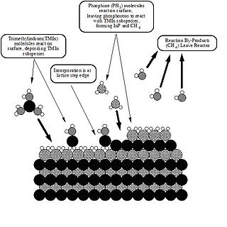
Metalorganic vapour-phase epitaxy (MOVPE), also known as organometallic vapour-phase epitaxy (OMVPE) or metalorganic chemical vapour deposition (MOCVD), is a chemical vapour deposition method used to produce single- or polycrystalline thin films. It is a process for growing crystalline layers to create complex semiconductor multilayer structures. In contrast to molecular-beam epitaxy (MBE), the growth of crystals is by chemical reaction and not physical deposition. This takes place not in vacuum, but from the gas phase at moderate pressures. As such, this technique is preferred for the formation of devices incorporating thermodynamically metastable alloys, and it has become a major process in the manufacture of optoelectronics, such as Light-emitting diodes, its most widespread application. It was first demonstrated in 1967 at North American Aviation Autonetics Division in Anaheim CA by Harold M. Manasevit.

<span class="mw-page-title-main">Thermal oxidation</span> Process creating a thin layer of (usually) silicon dioxide

In microfabrication, thermal oxidation is a way to produce a thin layer of oxide on the surface of a wafer. The technique forces an oxidizing agent to diffuse into the wafer at high temperature and react with it. The rate of oxide growth is often predicted by the Deal–Grove model. Thermal oxidation may be applied to different materials, but most commonly involves the oxidation of silicon substrates to produce silicon dioxide.

<span class="mw-page-title-main">Metal gate</span>

A metal gate, in the context of a lateral metal–oxide–semiconductor (MOS) stack, is the gate electrode separated by an oxide from the transistor's channel – the gate material is made from a metal. In most MOS transistors since about the mid-1970s, the "M" for metal has been replaced by polysilicon, but the name remained.

Adhesive bonding describes a wafer bonding technique with applying an intermediate layer to connect substrates of different types of materials. Those connections produced can be soluble or insoluble. The commercially available adhesive can be organic or inorganic and is deposited on one or both substrate surfaces. Adhesives, especially the well-established SU-8, and benzocyclobutene (BCB), are specialized for MEMS or electronic component production.

<span class="mw-page-title-main">Vapor–liquid–solid method</span> Mechanism to grow nano wires

The vapor–liquid–solid method (VLS) is a mechanism for the growth of one-dimensional structures, such as nanowires, from chemical vapor deposition. The growth of a crystal through direct adsorption of a gas phase on to a solid surface is generally very slow. The VLS mechanism circumvents this by introducing a catalytic liquid alloy phase which can rapidly adsorb a vapor to supersaturation levels, and from which crystal growth can subsequently occur from nucleated seeds at the liquid–solid interface. The physical characteristics of nanowires grown in this manner depend, in a controllable way, upon the size and physical properties of the liquid alloy.

<span class="mw-page-title-main">Copper indium gallium selenide solar cell</span>

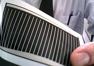
A copper indium gallium selenide solar cell is a thin-film solar cell used to convert sunlight into electric power. It is manufactured by depositing a thin layer of copper indium gallium selenide solid solution on glass or plastic backing, along with electrodes on the front and back to collect current. Because the material has a high absorption coefficient and strongly absorbs sunlight, a much thinner film is required than of other semiconductor materials.

Thermocompression bonding describes a wafer bonding technique and is also referred to as diffusion bonding, pressure joining, thermocompression welding or solid-state welding. Two metals, e.g. gold-gold (Au), are brought into atomic contact applying force and heat simultaneously. The diffusion requires atomic contact between the surfaces due to the atomic motion. The atoms migrate from one crystal lattice to the other one based on crystal lattice vibration. This atomic interaction sticks the interface together. The diffusion process is described by the following three processes:

<span class="mw-page-title-main">Crystalline silicon</span> Semiconducting material used in solar cell technology

Crystalline silicon or (c-Si) Is the crystalline forms of silicon, either polycrystalline silicon, or monocrystalline silicon. Crystalline silicon is the dominant semiconducting material used in photovoltaic technology for the production of solar cells. These cells are assembled into solar panels as part of a photovoltaic system to generate solar power from sunlight.

<span class="mw-page-title-main">Solar cell research</span> Research in the field of photovoltaics

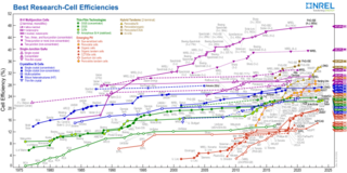
There are currently many research groups active in the field of photovoltaics in universities and research institutions around the world. This research can be categorized into three areas: making current technology solar cells cheaper and/or more efficient to effectively compete with other energy sources; developing new technologies based on new solar cell architectural designs; and developing new materials to serve as more efficient energy converters from light energy into electric current or light absorbers and charge carriers.

Direct bonding, or fusion bonding, describes a wafer bonding process without any additional intermediate layers. The bonding process is based on chemical bonds between two surfaces of any material possible meeting numerous requirements. These requirements are specified for the wafer surface as sufficiently clean, flat and smooth. Otherwise unbonded areas so called voids, i.e. interface bubbles, can occur.

Anodic bonding is a wafer bonding process to seal glass to either silicon or metal without introducing an intermediate layer; it is commonly used to seal glass to silicon wafers in electronics and microfluidics. This bonding technique, also known as field assisted bonding or electrostatic sealing, is mostly used for connecting silicon/glass and metal/glass through electric fields. The requirements for anodic bonding are clean and even wafer surfaces and atomic contact between the bonding substrates through a sufficiently powerful electrostatic field. Also necessary is the use of borosilicate glass containing a high concentration of alkali ions. The coefficient of thermal expansion (CTE) of the processed glass needs to be similar to those of the bonding partner.

Glass frit bonding, also referred to as glass soldering or seal glass bonding, describes a wafer bonding technique with an intermediate glass layer. It is a widely used encapsulation technology for surface micro-machined structures, e.g., accelerometers or gyroscopes. This technique utilizes low melting-point glass and therefore provides various advantages including that viscosity of glass decreases with an increase of temperature. The viscous flow of glass has effects to compensate and planarize surface irregularities, convenient for bonding wafers with a high roughness due to plasma etching or deposition. A low viscosity promotes hermetically sealed encapsulation of structures based on a better adaption of the structured shapes. Further, the coefficient of thermal expansion (CTE) of the glass material is adapted to silicon. This results in low stress in the bonded wafer pair. The glass has to flow and wet the soldered surfaces well below the temperature where deformation or degradation of either of the joined materials or nearby structures occurs. The usual temperature of achieving flowing and wetting is between 450 and 550 °C.

Reactive bonding describes a wafer bonding procedure using highly reactive nanoscale multilayer systems as an intermediate layer between the bonding substrates. The multilayer system consists of two alternating different thin metallic films. The self-propagating exothermic reaction within the multilayer system contributes the local heat to bond the solder films. Based on the limited temperature the substrate material is exposed, temperature-sensitive components and materials with different CTEs, i.e. metals, polymers and ceramics, can be used without thermal damage.

Transient liquid phase diffusion bonding (TLPDB) is a joining process that has been applied for bonding many metallic and ceramic systems which cannot be bonded by conventional fusion welding techniques. The bonding process produces joints with a uniform composition profile, tolerant of surface oxides and geometrical defects. The bonding technique has been exploited in a wide range of applications, from the production and repair of turbine engines in the aerospace industry, to nuclear power plants, and in making connections to integrated circuit dies as a part of the microelectronics industry.

References

  1. 1 2 3 4 5 6 7 8 9 10 11 Lin, Y.-C.; Baum M.; Haubold, M.; Fromel J.; Wiemer, M.; Gessner T.; Esashi, M. (2009). "Development and evaluation of AuSi eutectic wafer bonding". Solid-State Sensors, Actuators and Microsystems Conference, 2009. TRANSDUCERS 2009. International. pp. 244–247. doi:10.1109/SENSOR.2009.5285519.
  2. 1 2 Farrens, S.; Sood, S. (2008). "Wafer Level Packaging: Balancing Device Requirements and Materials Properties". IMAPS. International Microelectronics and Packaging Society. Archived from the original on 2011-09-25. Retrieved 2011-05-15.
  3. Venkatasubramanian, Rama (1992). "High Quality Eutectic-Metal-Bonded AlGaAs-GaAs Thin Films on Si Substrates". Appl. Phys. Lett. 60 (7): 886–889. Bibcode:1992ApPhL..60..886V. doi:10.1063/1.106494.
  4. Venkatasubramanian, Rama (1994). "Optoelectronic Properties of Eutectic-Metal-Bonded (EMB) GaAs-AlGaAs Structures on Si Substrates". Solid State Electronics. 37 (11): 1809–1815. Bibcode:1994SSEle..37.1809V. doi:10.1016/0038-1101(94)90171-6.
  5. 1 2 3 4 G. Gerlach; W. Dötzel (2008). Ronald Pething (ed.). Introduction to Microsystem Technology: A Guide for Students (Wiley Microsystem and Nanotechnology). Wiley Publishing. ISBN   978-0-470-05861-9.
  6. 1 2 3 4 5 R. F. Wolffenbuttel (1997). "Low-temperature intermediate Au-Si wafer bonding; eutectic or silicide bond". Sensors and Actuators A: Physical. 62 (1–3): 680–686. doi:10.1016/S0924-4247(97)01550-1.
  7. Farrens, S. (2008). Latest Metal Technologies for 3D Integration and MEMS Wafer Level Bonding (Report). SUSS MicroTec Inc.
  8. Matijasevic, G.S.; Lee C.C.; Wang, C.Y. (1993). "Au-Sn alloy phase diagram and properties related to its use as a bonding medium". Thin Solid Films. 223 (2): 276–287. Bibcode:1993TSF...223..276M. doi:10.1016/0040-6090(93)90533-U.
  9. 1 2 Sood, S.; Farrens S.; Pinker, R.; Xie J.; Cataby, W. (2010). "Al-Ge Eutectic Wafer Bonding and Bond Characterization for CMOS Compatible Wafer Packaging". ECS Transactions. 33 (4): 93–101. Bibcode:2010ECSTr..33d..93S. doi:10.1149/1.3483497.
  10. 1 2 Lani, S.; Bosseboeuf, A.; Belier, B.; Clerc, C.; Gousset, C.; Aubert, J. (2006). "Gold metallizations for eutectic bonding of silicon wafers". Microsystem Technologies. 12 (10–11): 1021–1025. doi:10.1007/s00542-006-0228-6.
  11. M. Wiemer; J. Frömel; T. Gessner (2003). "Trends der Technologieentwicklung im Bereich Waferbonden". In W. Dötzel (ed.). 6. Chemnitzer Fachtagung Mikromechanik & Mikroelektronik. Vol. 6. Technische Universität Chemnitz. pp. 178–188.
  12. 1 2 3 Farrens, S. (2008). "Wafer-Bonding Technologies and Strategies for 3D ICs. Chapter 4". In Tan, C. S.; Gutmann, R. J.; Reif, L. R. (eds.). Wafer Level 3-D ICs Process Technology. Integrated Circuits and Systems. Springer US. pp. 49–85. doi:10.1007/978-0-387-76534-1. ISBN   978-0-387-76532-7.
  13. Schneider, A.; Rank H.; Müller-Fiedler, R.; Wittler O.; Reichl, H. (2009). "Stabilitätsbewertung eutektisch gebondeter Sensorstrukturen auf Waferlevel". In Hermann, G. (ed.). 9. Chemnitzer Fachtagung Mikromechanik & Mikroelektronik. pp. 51–56.
  14. Yost, F. (1974). "Ultimate strength and morphological structure of eutectic bonds". Journal of Electronic Materials. 3 (2): 353–369. Bibcode:1974JEMat...3..353Y. doi:10.1007/BF02652947.
  15. Cheng, Y.T.; Lin L.; Najafi, K. (2000). "Localized silicon fusion and eutectic bonding for MEMS fabrication and packaging". Journal of Microelectromechanical Systems. 9 (1): 3–8. doi:10.1109/84.825770.
  16. Kim, J.; Cheng, Y.-T.; Chiao, M.; Lin, L. (2007). "Packaging and Reliability Issues in Micro/Nano Systems". In Bhushan, B. (ed.). Springer Handbook of Nanotechnology. Springer Berlin Heidelberg. pp. 1777–1806. Bibcode:2007shnt.book.....B. doi:10.1007/978-3-540-29857-1. ISBN   978-3-540-29855-7.
  17. 1 2 3 4 R. F. Wolffenbuttel; K. D. Wise (1994). "Low-temperature silicon wafer-to-wafer bonding using gold at eutectic temperature" (PDF). Sensors and Actuators A: Physical. 43 (1–3): 223–229. doi:10.1016/0924-4247(93)00653-L. hdl: 2027.42/31608 .