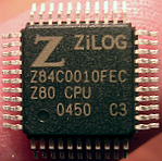
In microelectronics, a dual in-line package, or dual in-line pin package (DIPP) is an electronic component package with a rectangular housing and two parallel rows of electrical connecting pins. The package may be through-hole mounted to a printed circuit board (PCB) or inserted in a socket. The dual-inline format was invented by Don Forbes, Rex Rice and Bryant Rogers at Fairchild R&D in 1964, when the restricted number of leads available on circular transistor-style packages became a limitation in the use of integrated circuits. Increasingly complex circuits required more signal and power supply leads ; eventually microprocessors and similar complex devices required more leads than could be put on a DIP package, leading to development of higher-density chip carriers. Furthermore, square and rectangular packages made it easier to route printed-circuit traces beneath the packages.

A printed circuit board (PCB) mechanically supports and electrically connects electronic components or electrical components using conductive tracks, pads and other features etched from one or more sheet layers of copper laminated onto and/or between sheet layers of a non-conductive substrate. Components are generally soldered onto the PCB to both electrically connect and mechanically fasten them to it.
A QFP or Quad Flat Package is a surface-mounted integrated circuit package with "gull wing" leads extending from each of the four sides. Socketing such packages is rare and through-hole mounting is not possible. Versions ranging from 32 to 304 pins with a pitch ranging from 0.4 to 1.0 mm are common. Other special variants include low-profile QFP (LQFP) and thin QFP (TQFP).

Wave soldering is a bulk soldering process used in the manufacture of printed circuit boards. The circuit board is passed over a pan of molten solder in which a pump produces an upwelling of solder that looks like a standing wave. As the circuit board makes contact with this wave, the components become soldered to the board. Wave soldering is used for both through-hole printed circuit assemblies, and surface mount. In the latter case, the components are glued onto the surface of a printed circuit board (PCB) by placement equipment, before being run through the molten solder wave. Wave soldering is mainly used in soldering of through hole components.

Reflow soldering is a process in which a solder paste is used to temporarily attach one or thousands of tiny electrical components to their contact pads, after which the entire assembly is subjected to controlled heat. The solder paste reflows in a molten state, creating permanent solder joints. Heating may be accomplished by passing the assembly through a reflow oven or under an infrared lamp or by soldering individual joints [unconventionally] with a desoldering hot air pencil.
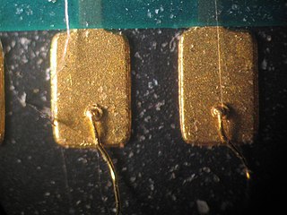
In electronics, a lead is an electrical connection consisting of a length of wire or a metal pad that is designed to connect two locations electrically. Leads are used for many purposes, including: transfer of power; testing of an electrical circuit to see if it is working, using a test light or a multimeter; transmitting information, as when the leads from an electrocardiograph are attached to a person's body to transmit information about their heart rhythm; and sometimes to act as a heatsink. The tiny leads coming off through-hole electronic components are also often called "pins"; in ball grid array packages, they are in form of small spheres, and are therefore called "balls".
A via or VIA is an electrical connection between layers in a physical electronic circuit that goes through the plane of one or more adjacent layers. To ensure via robustness, IPC sponsored a round-robin exercise that developed a time to failure calculator.
Solder paste is a material used in the manufacture of printed circuit boards to connect surface mount components to pads on the board. It is also possible to solder through hole pin in paste components by printing solder paste in/over the holes. The paste initially adheres components in place by being sticky, it is then heated melting the paste and forming a mechanical bond as well as an electrical connection. The paste is applied to the board by jet printing, stencil printing or syringe and then the components are put in place by a pick-and-place machine or by hand.

Flat no-leads packages such as quad-flat no-leads (QFN) and dual-flat no-leads (DFN) physically and electrically connect integrated circuits to printed circuit boards. Flat no-leads, also known as micro leadframe (MLF) and SON, is a surface-mount technology, one of several package technologies that connect ICs to the surfaces of PCBs without through-holes. Flat no-lead is a near chip scale plastic encapsulated package made with a planar copper lead frame substrate. Perimeter lands on the package bottom provide electrical connections to the PCB. Flat no-lead packages include an exposed thermal pad to improve heat transfer out of the IC. Heat transfer can be further facilitated by metal vias in the thermal pad. The QFN package is similar to the quad-flat package (QFP), and a ball grid array (BGA).

Perfboard is a material for prototyping electronic circuits. It is a thin, rigid sheet with holes pre-drilled at standard intervals across a grid, usually a square grid of 0.1 inches (2.54 mm) spacing. These holes are ringed by round or square copper pads, though bare boards are also available. Inexpensive perfboard may have pads on only one side of the board, while better quality perfboard can have pads on both sides. Since each pad is electrically isolated, the builder makes all connections with either wire wrap or miniature point to point wiring techniques. Discrete components are soldered to the prototype board such as resistors, capacitors, and integrated circuits. The substrate is typically made of paper laminated with phenolic resin or a fiberglass-reinforced epoxy laminate (FR-4).
Automated optical inspection (AOI) is an automated visual inspection of printed circuit board (PCB) manufacture where a camera autonomously scans the device under test for both catastrophic failure and quality defects. It is commonly used in the manufacturing process because it is a non-contact test method. It is implemented at many stages through the manufacturing process including bare board inspection, solder paste inspection (SPI), pre-reflow and post-reflow as well as other stages.

Bead probe technology (BPT) is technique used to provide electrical access to printed circuit board (PCB) circuitry for performing in-circuit testing (ICT). It makes use of small beads of solder placed onto the board's traces to allow measuring and controlling of the signals using a test probe. This permits test access to boards on which standard ICT test pads are not feasible due to space constraints.
Microvias are used as the interconnects between layers in high density interconnect (HDI) substrates and printed circuit boards (PCBs) to accommodate the high input/output (I/O) density of advanced packages. Driven by portability and wireless communications, the electronics industry strives to produce affordable, light, and reliable products with increased functionality. At the electronic component level, this translates to components with increased I/Os with smaller footprint areas, and on the printed circuit board and package substrate level, to the use of high density interconnects (HDIs).
A semiconductor package is a metal, plastic, glass, or ceramic casing containing one or more discrete semiconductor devices or integrated circuits. Individual components are fabricated on semiconductor wafers before being diced into die, tested, and packaged. The package provides a means for connecting the package to the external environment, such as printed circuit board, via leads such as lands, balls, or pins; and protection against threats such as mechanical impact, chemical contamination, and light exposure. Additionally, it helps dissipate heat produced by the device, with or without the aid of a heat spreader. There are thousands of package types in use. Some are defined by international, national, or industry standards, while others are particular to an individual manufacturer.
Pad cratering is a mechanically induced fracture in the resin between copper foil and outermost layer of fiberglass of a printed circuit board (PCB). It may be within the resin or at the resin to fiberglass interface.