
An integrated circuit is a set of electronic circuits on one small flat piece of semiconductor material, usually silicon. Large numbers of miniaturized transistors and other electronic components are integrated together on the chip. This results in circuits that are orders of magnitude smaller, faster, and less expensive than those constructed of discrete components, allowing a large transistor count.

In microelectronics, a dual in-line package is an electronic component package with a rectangular housing and two parallel rows of electrical connecting pins. The package may be through-hole mounted to a printed circuit board (PCB) or inserted in a socket. The dual-inline format was invented by Don Forbes, Rex Rice and Bryant Rogers at Fairchild R&D in 1964, when the restricted number of leads available on circular transistor-style packages became a limitation in the use of integrated circuits. Increasingly complex circuits required more signal and power supply leads ; eventually microprocessors and similar complex devices required more leads than could be put on a DIP package, leading to development of higher-density chip carriers. Furthermore, square and rectangular packages made it easier to route printed-circuit traces beneath the packages.

A ball grid array (BGA) is a type of surface-mount packaging used for integrated circuits. BGA packages are used to permanently mount devices such as microprocessors. A BGA can provide more interconnection pins than can be put on a dual in-line or flat package. The whole bottom surface of the device can be used, instead of just the perimeter. The traces connecting the package's leads to the wires or balls which connect the die to package are also on average shorter than with a perimeter-only type, leading to better performance at high speeds.

Surface-mount technology (SMT), originally called planar mounting, is a method in which the electrical components are mounted directly onto the surface of a printed circuit board (PCB). An electrical component mounted in this manner is referred to as a surface-mount device (SMD). In industry, this approach has largely replaced the through-hole technology construction method of fitting components, in large part because SMT allows for increased manufacturing automation which reduces cost and improves quality. It also allows for more components to fit on a given area of substrate. Both technologies can be used on the same board, with the through-hole technology often used for components not suitable for surface mounting such as large transformers and heat-sinked power semiconductors.

A pin grid array (PGA) is a type of integrated circuit packaging. In a PGA, the package is square or rectangular, and the pins are arranged in a regular array on the underside of the package. The pins are commonly spaced 2.54 mm (0.1") apart, and may or may not cover the entire underside of the package.

The zig-zag in-line package (ZIP) is a packaging technology for integrated circuits. It was intended as a replacement for dual in-line packaging. A ZIP is an integrated circuit encapsulated in a slab of plastic with 16, 20, 28 or 40 pins, measuring about 3 mm x 30 mm x 10 mm. The package's pins protrude in two rows from one of the long edges. The two rows are staggered by 1.27 mm (0.05"), giving them a zig-zag appearance, and allowing them to be spaced more closely than a rectangular grid would allow. The pins are inserted into holes in a printed circuit board, with the packages standing at right-angles to the board, allowing them to be placed closer together than DIPs of the same size. ZIPs have now been superseded by surface-mount packages such as the thin small-outline packages (TSOPs), but are still in use. The quad in-line package uses a similar staggered semiconductor package design.

Integrated circuit packaging is the final stage of semiconductor device fabrication, in which the die is encapsulated in a supporting case that prevents physical damage and corrosion. The case, known as a "package", supports the electrical contacts which connect the device to a circuit board.

In computer hardware, a CPU socket or CPU slot contains one or more mechanical components providing mechanical and electrical connections between a microprocessor and a printed circuit board (PCB). This allows for placing and replacing the central processing unit (CPU) without soldering.

The land grid array (LGA) is a type of surface-mount packaging for integrated circuits (ICs) that is notable for having the pins on the socket — as opposed to pins on the integrated circuit, known as a pin grid array (PGA). An LGA can be electrically connected to a printed circuit board (PCB) either by the use of a socket or by soldering directly to the board.
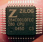
A quad flat package (QFP) is a surface-mounted integrated circuit package with "gull wing" leads extending from each of the four sides. Socketing such packages is rare and through-hole mounting is not possible. Versions ranging from 32 to 304 pins with a pitch ranging from 0.4 to 1.0 mm are common. Other special variants include low-profile QFP (LQFP) and thin QFP (TQFP).

Solid Logic Technology (SLT) was IBM's method for hybrid packaging of electronic circuitry introduced in 1964 with the IBM System/360 series of computers and related machines. IBM chose to design custom hybrid circuits using discrete, flip chip-mounted, glass-encapsulated transistors and diodes, with silk-screened resistors on a ceramic substrate, forming an SLT module. The circuits were either encapsulated in plastic or covered with a metal lid. Several of these SLT modules were then mounted on a small multi-layer printed circuit board to make an SLT card. Each SLT card had a socket on one edge that plugged into pins on the computer's backplane.
In electronics, a lead is an electrical connection consisting of a length of wire or a metal pad that is designed to connect two locations electrically. Leads are used for many purposes, including: transfer of power; testing of an electrical circuit to see if it is working, using a test light or a multimeter; transmitting information, as when the leads from an electrocardiograph are attached to a person's body to transmit information about their heart rhythm; and sometimes to act as a heatsink. The tiny leads coming off through-hole electronic components are also often called pins; in ball grid array packages, they are in form of small spheres, and are therefore called "balls".

A small outline integrated circuit (SOIC) is a surface-mounted integrated circuit (IC) package which occupies an area about 30–50% less than an equivalent dual in-line package (DIP), with a typical thickness being 70% less. They are generally available in the same pin-outs as their counterpart DIP ICs. The convention for naming the package is SOIC or SO followed by the number of pins. For example, a 14-pin 4011 would be housed in an SOIC-14 or SO-14 package.

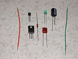
The TO-220 is a style of electronic package used for high-powered, through-hole components with 0.1 inches (2.54 mm) pin spacing. The "TO" designation stands for "transistor outline". TO-220 packages have three leads. Similar packages with two, four, five or seven leads are also manufactured. A notable characteristic is a metal tab with a hole, used to mount the case to a heatsink, allowing the component to dissipate more heat than one constructed in a TO-92 case. Common TO-220-packaged components include discrete semiconductors such as transistors and silicon-controlled rectifiers, as well as integrated circuits.

Flat no-leads packages such as quad-flat no-leads (QFN) and dual-flat no-leads (DFN) physically and electrically connect integrated circuits to printed circuit boards. Flat no-leads, also known as micro leadframe (MLF) and SON, is a surface-mount technology, one of several package technologies that connect ICs to the surfaces of PCBs without through-holes. Flat no-lead is a near chip scale plastic encapsulated package made with a planar copper lead frame substrate. Perimeter lands on the package bottom provide electrical connections to the PCB. Flat no-lead packages usually, but not always, include an exposed thermally conductive pad to improve heat transfer out of the IC. Heat transfer can be further facilitated by metal vias in the thermal pad. The QFN package is similar to the quad-flat package (QFP), and a ball grid array (BGA).

In electronics, TO-3 is a designation for a standardized metal semiconductor package used for power semiconductors, including transistors, silicon controlled rectifiers, and, integrated circuits. TO stands for "Transistor Outline" and relates to a series of technical drawings produced by JEDEC.

Flatpack is a US military standardized printed-circuit-board surface-mount-component package. The military standard MIL-STD-1835C defines: Flat package (FP). A rectangular or square package with leads parallel to base plane attached on two opposing sides of the package periphery.
A semiconductor package is a metal, plastic, glass, or ceramic casing containing one or more discrete semiconductor devices or integrated circuits. Individual components are fabricated on semiconductor wafers before being diced into die, tested, and packaged. The package provides a means for connecting it to the external environment, such as printed circuit board, via leads such as lands, balls, or pins; and protection against threats such as mechanical impact, chemical contamination, and light exposure. Additionally, it helps dissipate heat produced by the device, with or without the aid of a heat spreader. There are thousands of package types in use. Some are defined by international, national, or industry standards, while others are particular to an individual manufacturer.

In microelectronics, a quad in-line package, is an electronic component package with a rectangular housing and four parallel rows of electrical connecting pins. The package may be through-hole mounted to a printed circuit board (PCB) or inserted in a socket. Rockwell used a QIP with 42 leads formed into staggered rows for their PPS-4 microprocessor family introduced in 1973, and other microprocessors and microcontrollers, some with higher lead counts, through the early 1990s.


